Method for preparing graphene by adopting electronic beam irradiation technology
A technology of electron beam irradiation and graphene, which is applied in the field of preparation of graphene and graphene by electron beam irradiation technology. The effect of mild preparation conditions and simple operation
- Summary
- Abstract
- Description
- Claims
- Application Information
AI Technical Summary
Problems solved by technology
Method used
Image
Examples
Embodiment 1
[0026] 1. Preparation of PMMA fiber
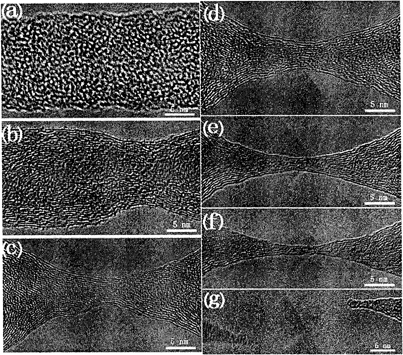
[0027] The nanofiber of PMMA is prepared by electrospinning method: PMMA is dissolved in the mixed solution of chlorobenzene and DMF (chlorobenzene and DMF are mixed with the volume ratio of 1: 1), the operating voltage at electrospinning is 25kV, working distance Under the condition that the distance between the substrate and the needle head is 12 cm, the fiber is deposited on the micro-grid, and the diameter of the obtained nanofiber is between 2 and 50 nanometers. To remove the solvent, the as-prepared PMMA nanofibers were annealed at 50 °C for 30 min.
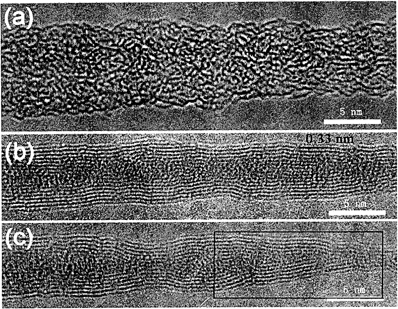
[0028] 2. Preparation of 10nm wide 15-layer graphene
[0029] Electron beam irradiation was performed on a high-resolution transmission electron microscope. The working voltage is 200kV, and the strength is 5×10 6 enm -2 the s -1 , the beam spot size (diameter) is 10nm electron beam irradiation 15nm diameter PMMA nanofiber 120s, obtains 15 layers, 10nm wide graphene parallel to ele...
Embodiment 2
[0031] 1. Preparation of PMMA fiber
[0032] With embodiment 1.
[0033] 2. Preparation of 10nm wide 7-layer graphene
[0034] Electron beam exposure was performed on a transmission electron microscope. The working voltage is 200kV, and the strength is 5×10 6 enm -2 the s -1 , the beam spot size (diameter) is 10nm electron beam irradiation 15nm diameter PMMA nanofiber 3 minutes, obtains 7 layers, 10nm wide graphene parallel to electron beam irradiation direction.
Embodiment 3
[0036] 1. Preparation of PMMA fiber
[0037] With embodiment 1.
[0038] 2. Preparation of 10nm wide 3-layer graphene
[0039] Electron beam exposure was performed on a transmission electron microscope. The working voltage is 200kV, and the strength is 5×10 6 enm -2 the s -1 , PMMA nanofibers with a diameter of 15 nm were irradiated with an electron beam with a diameter of 10 nm for 4 minutes to obtain three layers of graphene with a width of 10 nm parallel to the direction of the electron beam irradiation.
PUM
 Abstract
Description
Claims
Application Information

