Preparation method of CdTe film solar cell
A technology of solar cells and thin films, which is applied in the manufacture of circuits, electrical components, and final products. It can solve problems such as understanding and scattered CdTe solar cells, and achieve the effects of increasing effectiveness, reducing intermediate pollution links, and improving battery efficiency.
- Summary
- Abstract
- Description
- Claims
- Application Information
AI Technical Summary
Problems solved by technology
Method used
Image

Examples
Embodiment Construction
[0024] Carry out the preparation of CdTe thin film solar cell according to the following preparation process:
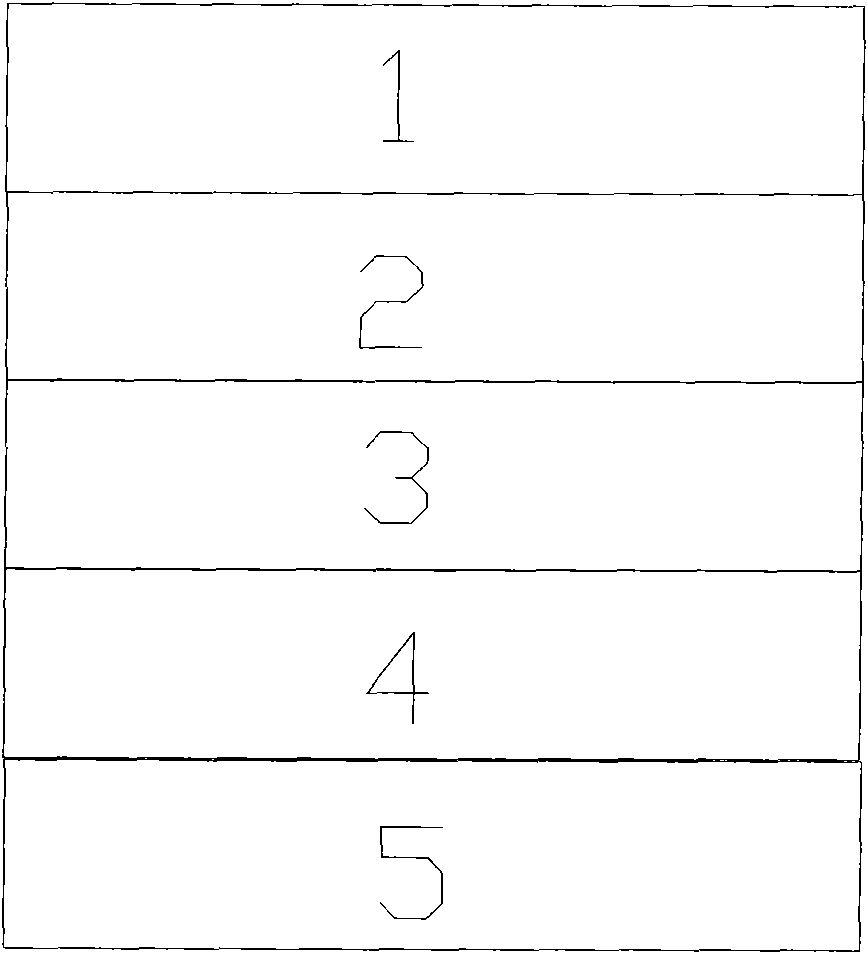
[0025] (1) Pretreatment of the transparent glass substrate 1: use 1713 glass as the deposition substrate 1. Ultrasonic cleaning with acetone for 10 minutes to remove surface grease, and then ultrasonic cleaning with deionized water for 10 minutes to remove impurities on the glass surface; finally, the glass is dried and placed in a pretreatment chamber, and the glass substrate 1 is cleaned with plasma.
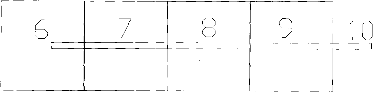
[0026] (2) Preparation of In 2 o 3 : F transparent conductive film 2: the transparent glass substrate 1 is transferred to the sample stage of the magnetron sputtering apparatus 9 by the mechanical arm 10, and the sputtering target material is high-purity In 2 o 3 . First use a vacuum pump to evacuate the sputtering chamber to 3Pa, then use a molecular pump to evacuate the reaction chamber to 1×10 -3 Pa. Infuse Ar gas and 5% CHF 3 , the flow rate is adjusted to...
PUM
 Abstract
Description
Claims
Application Information
PatSnap Eureka turns technology decisions into work you can execute. Powered by our Innovation Knowledge Graph, it runs expert workflows across engineering, life sciences, materials and intellectual property. Get your review-ready output in minutes.


