

Printable semiconductor structures and related methods of making and assembling
A semiconductor, structural technology, applied in the field of printable semiconductor structures and related manufacturing and assembly, which can solve the problems of damage, non-electronic characteristics of integrated electronic devices, cracking, etc.
- Summary
- Abstract
- Description
- Claims
- Application Information
AI Technical Summary
Problems solved by technology
Method used
Image

Examples
Embodiment 1
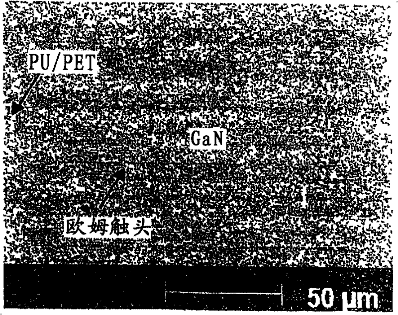
[0105] Example 1 Aligned GaAs line arrays for flexible transistors, diodes and circuits printed on plastic substrates
[0106] GaAs line-aligned arrays with integrated ohmic contacts produced from high-quality single-crystal wafers using photolithography and anisotropic chemical etching provide a promising transistor for use on flexible plastic substrates, Materials for Schottky diodes, logic gates, and even more complex circuits. These devices exhibit excellent electrical and mechanical properties, both of which are important for the emerging field of low-cost, large-area flexible electronics, often called macroelectronics.
[0107] Micro- and nano-scale wires, ribbons, platelets, etc. of single-crystalline inorganic semiconductors are attractive for functional devices (e.g., optical devices, optoelectronic devices, electronic devices, sensor devices, etc.) that can be used in many applications. The building block of force. For example, Si nanowires synthesized by a "bottom...
Embodiment 2
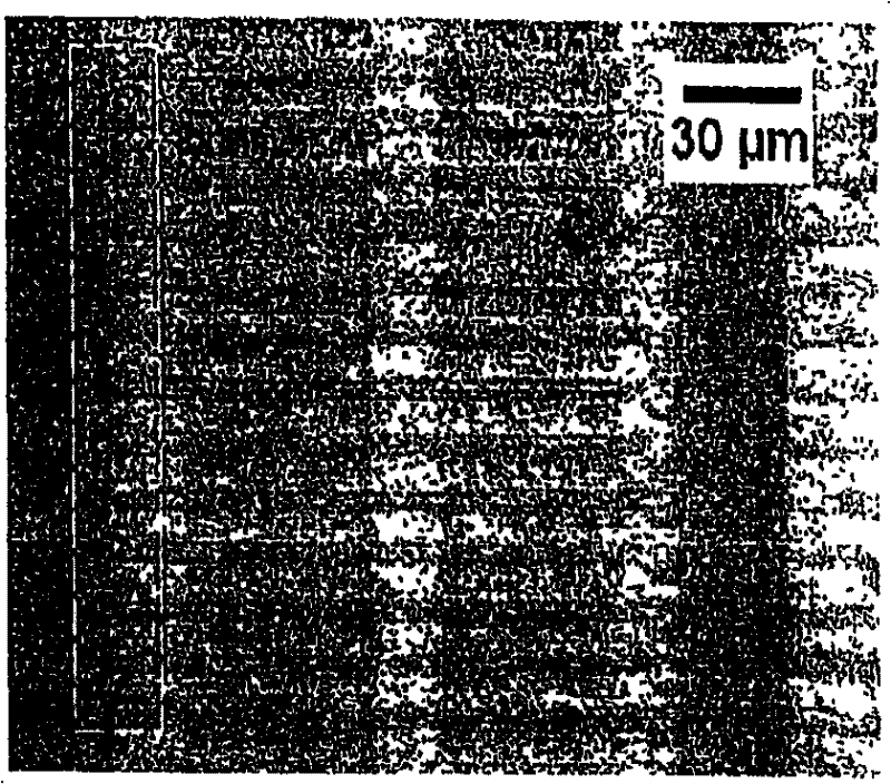
[0119] Example 2: Gigahertz operation of a mechanically flexible transistor on a flexible plastic substrate
[0120] The combined use of GaAs wires with ohmic contacts formed from bulk wafers, soft lithographic transfer printing techniques, and optimized device designs enables the formation of mechanically flexible transistors on low-cost plastic substrates with individual device speeds in the gigahertz range and with High mechanical bendability. The methods disclosed herein include materials that are fabricated with limited lithographic image forming resolution and registration in a simple layout. This example describes the electrical and mechanical properties of high performance transistors. These results are of great importance in certain applications including, but not limited to, high-speed communications and computing, and emerging types of large-area electronic systems ("macroelectronic devices").
[0121] Large-area flexible electronic systems (ie, macroelectronic de...
Embodiment 3
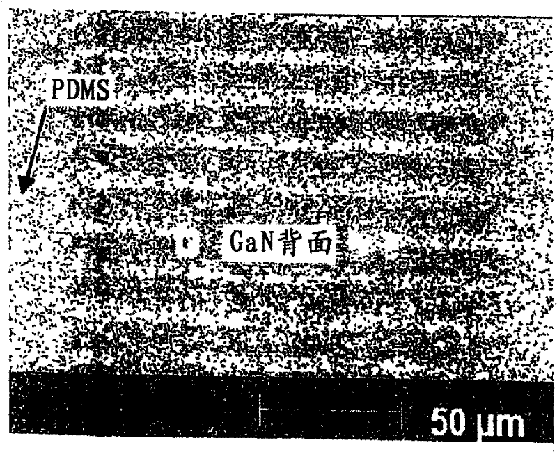
[0144] Example 3 Mechanically Flexible Thin Film Transistor Using Ultra-Thin Silicon Ribbons Harvested from Bulk Wafers This Example introduces a thin film transistor using an aligned array of thin (submicron) Aligned arrays of silicon thin (submicron) ribbons were produced by lithographic patterning and anisotropic etching of bulk silicon (111) wafers. Devices incorporating such ribbons printed onto thin plastic substrates showed good electrical properties as well as mechanical flexibility. Effective device mobility, as estimated in the linear region, up to 360cm 2 V -1 the s -1 and on / off ratio > 10 3 . These results represent an important advance in low-cost methods for fabricating large-area, high-performance, mechanically flexible electronic systems for structural health monitoring, sensors, displays, and other applications.
[0145]Confinement-related properties and wide-ranging form factors make low-dimensional materials promising new applications in electronics, p...
PUM
 Abstract
Description
Claims
Application Information