Optical adjacent correction method suitable for pixel array of image sensor

A technology of optical proximity correction and image sensor, which is applied to the original parts, optics, and image communication for opto-mechanical processing. Achieve the effect of shortening the production cycle, shortening the computing time and reducing the amount of data

Inactive Publication Date: 2010-02-10
ZHEJIANG UNIV
View PDF0 Cites 23 Cited by
  • Summary
  • Abstract
  • Description
  • Claims
  • Application Information

AI Technical Summary

Problems solved by technology

Most of the current CMOS image sensor pixel circuits share a set of readout circuits for multiple pixels, and the most common one is for four pixels to share a set of readout circuits (such as figure 1 shown), parallel pixel units are usually symmetrical on the layout (such as figure 2 As shown), there are strict requirements on the symmetry of the layout pattern, and the traditional OPC processing results are often asymmetrical, so it is difficult to ensure the symmetry of the lithography results on the silicon wafer

Method used


Image

  • Optical adjacent correction method suitable for pixel array of image sensor
  • Optical adjacent correction method suitable for pixel array of image sensor
  • Optical adjacent correction method suitable for pixel array of image sensor

Examples


Embodiment Construction

[0038]The present invention will be further described below in conjunction with accompanying drawing.

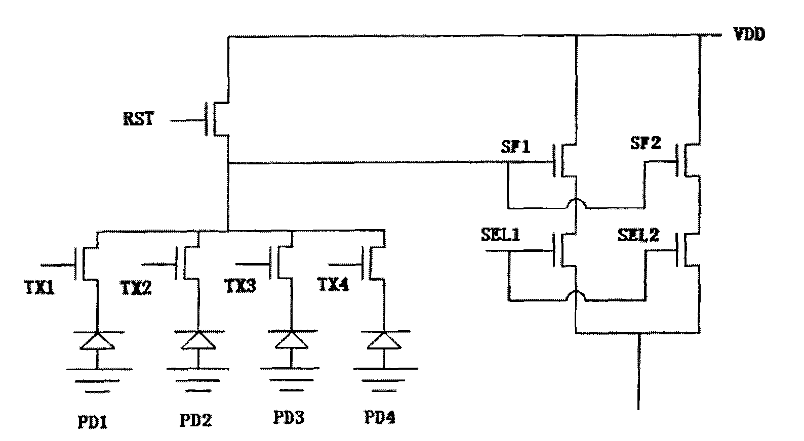
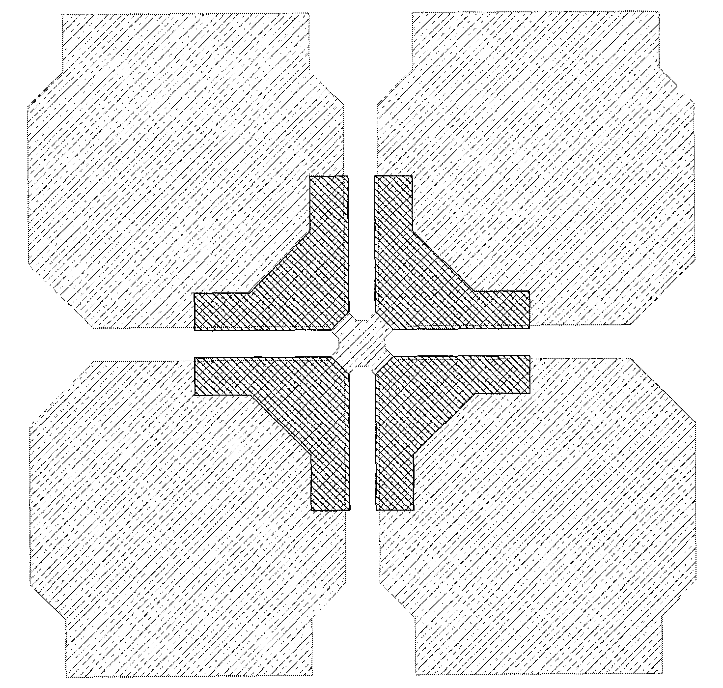
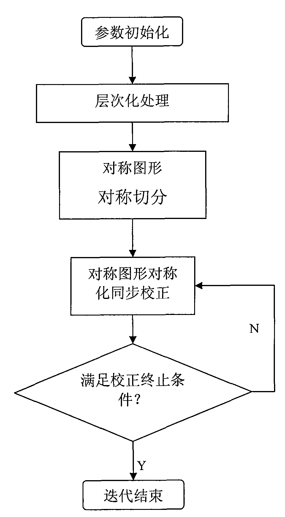
[0039] An optical proximity correction method suitable for image sensor pixel arrays, the process is as follows image 3 As shown, it includes parameter initialization, layout hierarchical processing, symmetrical segmentation of symmetrical graphics, and symmetric correction of symmetrical graphics. The specific steps are as follows:

[0040] 1) Parameter initialization:

[0041] Set up the simulation model for optical proximity correction,

[0042] Photolithographic mask pattern, GDSII input,

[0043] The feature size D of the photolithographic mask pattern,

[0044] The basic parameters of the lithography machine, λ, NA, σ; where: λ is the wavelength of the light source, NA is the numerical aperture of the optical system, and σ is the coherence coefficient of the illumination;

[0045] 2) Determine the interaction distance of graphics through the parameters of the opti...


PUM


Abstract

The invention discloses an optical adjacent correction method suitable for a pixel array of an image sensor, which comprises steps of parameter initialization, territory layering processing, symmetrical segmentation of a symmetrical pattern, symmetrization correction of the symmetrical pattern and the like. The method can guarantee the consistency of pixels and the symmetry of a photoetching result pattern, thus ensuring the performance of the pixel array, reducing the data volume of the optical adjacent correction result, obviously inhibiting ripple wave phenomenon in the deep sub-micron technology and various manufacturing defects of off-line, bridging, corner smoothing, line end indentation and the like caused by the ripple wave phenomenon, shortening the production period, and increasing the finished product ratio of a CMOS image sensor.

Description

technical field [0001] The invention relates to an optical proximity correction method suitable for an image sensor pixel array. Background technique [0002] Image sensor is a basic device for obtaining visual information. It can realize information acquisition, conversion and expansion of visual functions, and obtain rich image information. It is more and more widely used in modern social life. Currently, there are mainly two types of image sensors, charge-coupled device (Charge-Coupled Device, CCD) and complementary metal oxide field effect transistor (Complementary Metal Oxide Semiconductor, CMOS) image sensors. The research on these two types of image sensors started almost simultaneously in the late 1960s. However, due to the limitation of the technological level at that time, the imperfect performance of CMOS image sensors seriously affected the image quality, thus restricting its development and application. In the 1970s and 1980s, CCD image sensors dominated visibl...

Claims


Application Information

Patent Timeline
Patent Type & Authority Applications(China)
IPC IPC(8): G03F1/14G06F17/50H01L21/00H04N5/335G03F1/36
Inventor 林斌严晓浪赵立新史峥李杰孟庆薛江
Owner ZHEJIANG UNIV
Why Eureka
Try Eureka