Circuit device three-dimensional integrative method

A technology of circuit devices and three-dimensional integration, applied in chemical instruments and methods, circuits, electrical components, etc., can solve the problems of three-dimensional interconnection aspect ratio limitation, blind holes are sealed, etc., achieve high aspect ratio, avoid holes and Gap, the effect of high three-dimensional integration

Inactive Publication Date: 2010-02-10
TSINGHUA UNIV
View PDF0 Cites 10 Cited by
  • Summary
  • Abstract
  • Description
  • Claims
  • Application Information

AI Technical Summary

Problems solved by technology

[0006] After researching the existing technology, the inventors found that, based on the realization of the blind hole, since only Damascus plating can be used, it is easy to make the blind hole be sealed at the opening first, forming a hole inside the filled metal line
In order to ensure the reliability of the three-dimensional interconnection, the blind holes made on the substrate cannot be too deep, so the aspect ratio of realizing the three-dimensional interconnection of the substrate wafer is very limited
It is easy to fill the through-holes based on the implementation of through-holes, but in order to ensure the operability on the substrate wafer, the thickness of the single-layer substrate wafer often exceeds 200 microns. Although it has a high aspect ratio, it also limits Increased interconnect density

Method used


Image

  • Circuit device three-dimensional integrative method
  • Circuit device three-dimensional integrative method
  • Circuit device three-dimensional integrative method

Examples


Embodiment 1

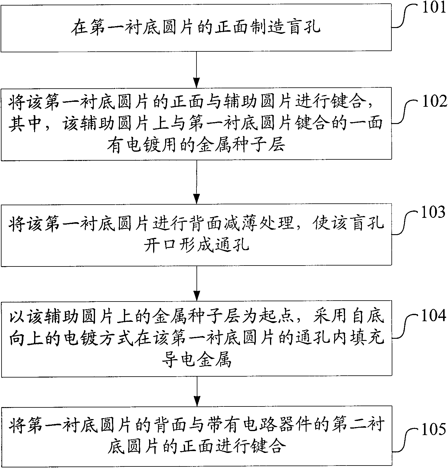
[0030] The embodiment of the present invention provides a method for three-dimensional interconnection of circuit devices, which can perform three-dimensional vertical interconnection of substrate wafers of circuit devices with high density and high aspect ratio, effectively realizing three-dimensional interconnection of circuit devices and 3D integration.

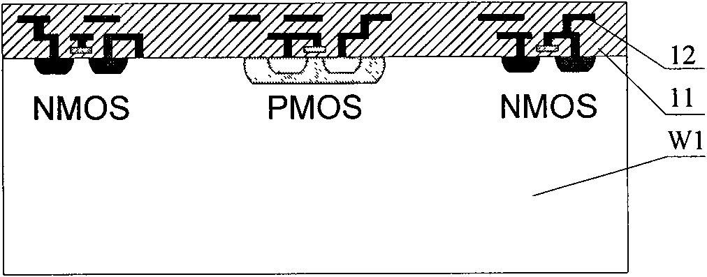
[0031] In this embodiment, the implementation of three-dimensional interconnection of substrate wafers of two-layer circuit devices is taken as an example for illustration. figure 1 Shown is the substrate wafer W1 used in this embodiment, which includes fabricated circuit devices, such as integrated circuits, MEMS devices, or microsensors; the substrate wafer W1 also includes : multilayer metal interconnection 12, and the interlayer dielectric layer or surface passivation layer 11 of the metal interconnection 12. Wherein, the material of the substrate wafer may be silicon, strained silicon, silicon germanium, gallium arse...

Embodiment 2

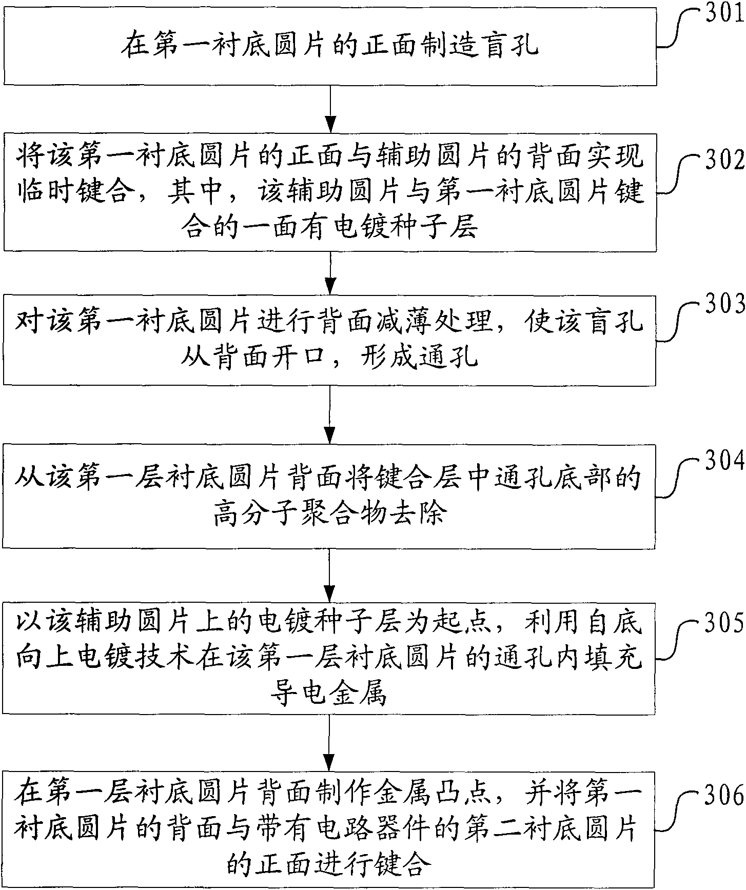
[0045] The embodiment of the present invention provides a method for three-dimensional integration of circuit devices, which can perform three-dimensional vertical interconnection of substrate wafers of circuit devices with high density and high aspect ratio, effectively realizing three-dimensional integration and three-dimensional integration of circuit devices. interconnection.

[0046] In this embodiment, the implementation of three-dimensional interconnection of substrate wafers of two-layer circuit devices is taken as an example for illustration. figure 1 Shown is the substrate wafer W1 used in this embodiment, which includes fabricated circuit devices, such as integrated circuits, MEMS devices, or microsensors; the substrate wafer W1 also includes : multilayer metal interconnection 12, and the interlayer dielectric layer or surface passivation layer 11 of the metal interconnection 12. Wherein, the material of the substrate wafer W1 may be silicon, strained silicon, sili...


PUM


Abstract

The invention discloses a circuit device three-dimensional integrative method, which comprises the following steps of: manufacturing a blind hole on the front side of a first substrate disc with the circuit device; bonding the front side of a first substrate disc and an auxiliary disc, carrying out back reduction processing on the first substrate disc, and causing an open mouth of the blind hole to form a through hole; using a metal seed layer on the auxiliary disc as a starting point and filling an electric conduction metal in the through hole in an electro-plating mode from bottom to top; and bonding the back side of the first substrate disc and the front side of a second substrate disc with the circuit device. In the embodiment of the invention, when the circuit device is integrated ina three-dimensional way, the blind hole is manufactured in the substrate disc with the circuit device and opened to form the through hole, and the metal is filled in the through hole by using the auxiliary disc in the electro-plating mode from bottom to top, thus avoiding a hole and a gap appearing on the electro-plated bind hole, realizing the three-dimensional interconnection of high density andhigh aspect ratio, and simultaneously reducing the technology difficulty of the three-dimensional integration and interconnection.

Description

technical field [0001] The invention relates to the field of integrated circuit manufacturing, in particular to a method for three-dimensional integration of circuit devices. Background technique [0002] Circuit devices, such as integrated circuits, sensors and MEMS (Micro-Electro-Mechanical System), have now developed to the stage of system-on-a-chip (SOC, System on a Chip), and the production of system-on-chip is adopted Technology can realize all the functions of the system on a single chip. One of the difficulties in the development of SOC is the compatibility of different manufacturing processes. In the process of making SOC, it may be necessary to use a variety of standard manufacturing processes, but the manufacturing methods and adoption of these manufacturing processes The substrate materials are different, and it is difficult to implement them on the same chip. Even if the substrate materials are the same, the manufacturing feasibility of each circuit module must ...

Claims


Application Information

Patent Timeline
Patent Type & Authority Applications(China)
IPC IPC(8): H01L21/48H01L21/50H01L21/60B81C1/00B81C3/00B81C5/00
Inventor 王喆垚宋崇申徐向明刘理天
Owner TSINGHUA UNIV
Why Eureka
Try Eureka