

Preparation method of solar microbattery based on random mesh carbon nanotube film
A technology of solar micro-battery and carbon nanotube thin film, which is applied in the manufacture of circuits, electrical components, and final products, etc., can solve the problems of complicated structure manufacturing process, unfavorable long-term stability of solar cell structure, etc., and achieves easy mass production and structure. Simple structure and high stability
- Summary
- Abstract
- Description
- Claims
- Application Information
AI Technical Summary
Problems solved by technology
Method used
Image

Examples
Embodiment 1
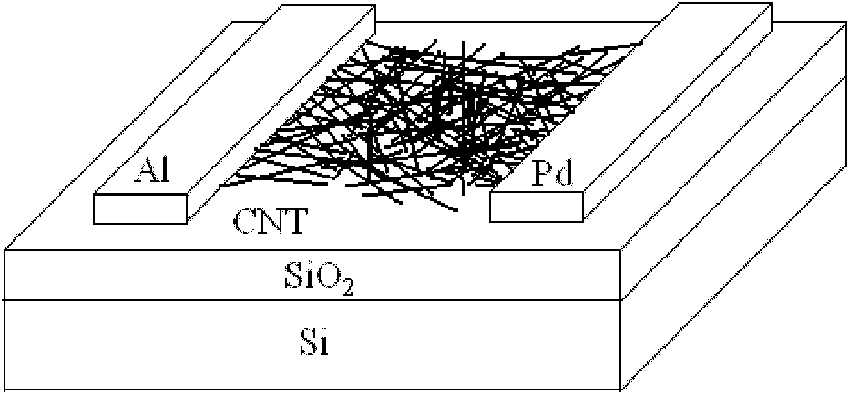
[0028] In this example, a self-assembly method is used to prepare a disordered network single-walled carbon nanotube film, and a disordered networked semiconducting single-walled carbon nanotube film is obtained by using a methane plasma etching method. A pair of symmetrical metal electrodes constitutes an asymmetric solar micro battery.
[0029] Soak the cleaned silicon wafer with a silicon dioxide layer on the surface in H 2 SO 4 and H 2 o 2 The surface of the silicon wafer is made hydrophilic in the mixed solution, where H 2 SO 4 and H 2 o 2 The ratio range is 2:1, the soaking time is 10 hours, and the soaking temperature is 80 degrees; then the silicon wafer cleaned by deionized water is soaked in the APS solution, so that the single-layer APS is modified to a hydrophilic carbon dioxide Silicon surface, immersion time is 10h, H in APS solution 2 The ratio range of O and APS is 100:1; then the silicon wafers cleaned with deionized water and dried are placed in a sus...
Embodiment 2
[0033] In this example, a self-assembly method is used to prepare a disordered network single-walled carbon nanotube film, and a disordered networked semiconducting single-walled carbon nanotube film is obtained by using a methane plasma etching method. A pair of symmetrical metal electrodes constitutes an asymmetric solar micro battery.
[0034] Soak the cleaned silicon wafer with a silicon dioxide layer on the surface in H 2 SO 4 and H 2 o 2 The surface of the silicon wafer is made hydrophilic in the mixed solution, where H 2 SO 4 and H 2 o 2 The ratio range is 6:1, the soaking time is 24 hours, and the soaking temperature is 100 degrees; then the silicon wafer cleaned by deionized water is soaked in the APS solution so that the single layer of APS is modified to the hydrophilic silica surface , soaking time is 24h, H in APS solution 2 The ratio range of O and APS is 10000:1; then the silicon wafers cleaned with deionized water and dried are placed in a suspension of...
Embodiment 3
[0038] In this example, a self-assembly method is used to prepare a disordered network single-walled carbon nanotube film, and a disordered networked semiconducting single-walled carbon nanotube film is obtained by using a methane plasma etching method. A pair of symmetrical metal electrodes constitutes an asymmetric solar micro battery.
[0039] Soak the cleaned silicon wafer with a silicon dioxide layer on the surface in H 2 SO 4 and H 2 o 2 The surface of the silicon wafer is made hydrophilic in the mixed solution, where H 2 SO 4 and H 2 o 2 The ratio range is 1:1, the soaking time is 2 hours, and the soaking temperature is 20 degrees; then the silicon wafer cleaned by deionized water is soaked in the APS solution so that the single layer of APS is modified to hydrophilic silica Surface, immersion time is 2h, H in APS solution 2 The ratio range of O and APS is 20:1; then the silicon wafers cleaned with deionized water and dried are placed in a suspension of single-w...
PUM
| Property | Measurement | Unit |
|---|---|---|
| concentration | aaaaa | aaaaa |
| concentration | aaaaa | aaaaa |
| concentration | aaaaa | aaaaa |
Abstract
Description
Claims
Application Information