Full-difference CMOS ultra wide band low-noise amplifier

A low-noise amplifier and ultra-wideband technology, applied in differential amplifiers, high-frequency amplifiers, improved amplifiers to expand bandwidth, etc., can solve the problems of large load inductance, large chip area, high power consumption, etc., and achieve small chip area, Effect of high gain and low power consumption

Inactive Publication Date: 2010-02-24
FUDAN UNIV
View PDF1 Cites 36 Cited by
  • Summary
  • Abstract
  • Description
  • Claims
  • Application Information

AI Technical Summary

Problems solved by technology

Since the gain of the LNA of this structure is proportional to the transconductance of the input common-source transistor, the requirement of broadband and high gain will inevitably lead to higher power consumption; in addition, in order to compensate the influence

Method used


Image

  • Full-difference CMOS ultra wide band low-noise amplifier
  • Full-difference CMOS ultra wide band low-noise amplifier
  • Full-difference CMOS ultra wide band low-noise amplifier

Examples


Embodiment Construction

[0040] Further describe the present invention below in conjunction with accompanying drawing.

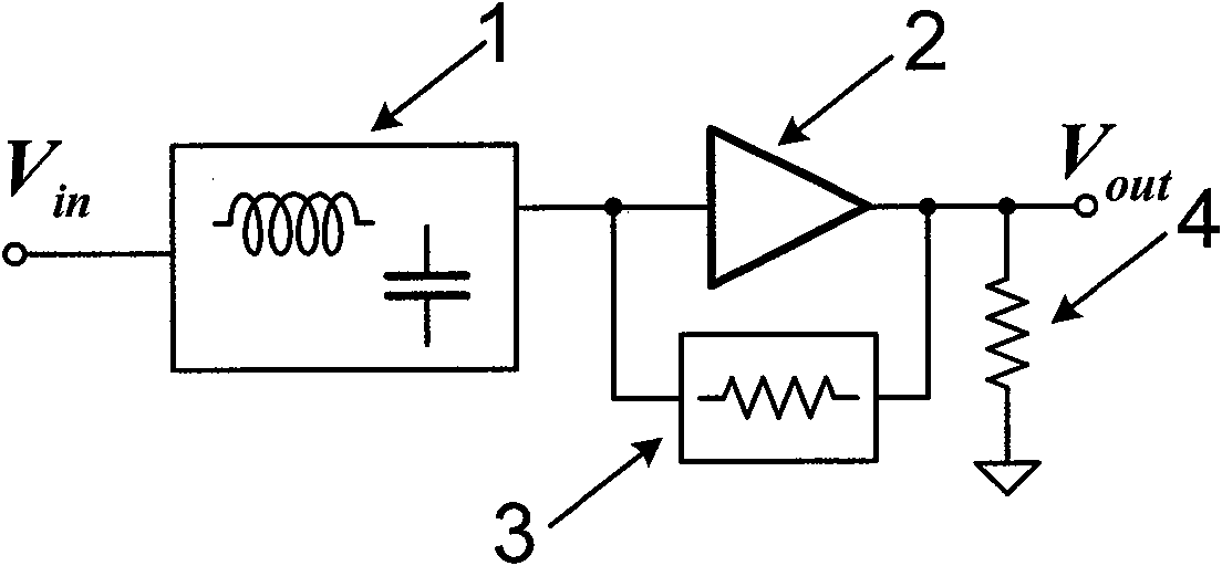
[0041] refer to figure 1 Shown is the structural block diagram of the CMOS ultra-wideband LNA of the present invention, which is composed of a matching stage 1, an amplification stage 2, a feedback stage 3 and a load stage 4 connected in sequence.

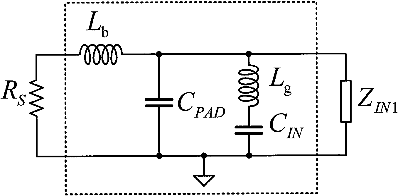
[0042] refer to figure 2 As shown, the matching network is composed of input matching stage 1 and feedback stage 3. The matching network is essentially a band-pass filter to achieve broadband input matching. Matching stage 1 can be regarded as a 2nd order LC network. where Rs is the resistance of the input signal source, L b is the bonding wire inductance of the chip pin, C PAD is the equivalent parasitic capacitance on the chip PAD, L g is the input transconductor gate inductance, C IN is the equivalent input capacitance of the input transconductor, Z IN1 is the equivalent input impedance seen from the feedback path, such as ...


PUM


Abstract

The invention relates to a full-difference CMOS ultra wide band low-noise amplifier which can be applied in the ultra wide band of 3.1-4.8GHz and 3.1-10.6GHz or can be applied in cognitive radio frequency front end of 900MHz-6GHz. The amplifier is based on common-source transconductance input and resistance negative feedback structure and is composed of a matching stage, an amplifying stage, a feedback stage and a load stage, wherein, the matching stage uses grid electrode inductance to tune wideband input impedance; the amplifying stage uses a current multiplexing common-source stage NMOS tube and a PMOS tube to serve as the input end, a common-grid electrode NMOS tube which is connected with the drain terminal output thereof is used as a current follower; an NMOS tube between an input NMOS tube grid electrode and a current follower NMOS tube drain electrode and resistance form a voltage-current type negative feedback circuit; the load stage uses resistance to load. The invention hassimple structure, occupies small chip area, has high gain and low power consumption and can satisfy the requirement of radio frequency front end of a wideband communication system.

Description

technical field [0001] The invention belongs to the field of radio frequency integrated circuits, and specifically relates to the design of a fully differential low noise amplifier with high gain, low noise and good input matching, especially for 3.1-4.8GHz, 3.1-10.6GHz ultra-wideband UWB radio frequency front-end or 900MHz~ 6GHz Cognitive Radio (SDR) RF front-end. Background technique [0002] UWB wireless communication technology and cognitive radio technology are currently research hotspots in academia and industry. Especially as a high-speed and low-power data communication method, UWB is expected to be widely used in the field of wireless communication. UWB wireless communication mainly includes three ways of UWB: carrierless pulse UWB (IR-UWB), direct sequence (DS-UWB) and multi-band OFDM (MB-OFDM) UWB. In either implementation, however, the RF receiver requires the use of a wideband LNA block. [0003] The low-noise amplifier is one of the most critical modules in ...

Claims


Application Information

Patent Timeline
IPC IPC(8): H03F3/19H03F3/45H03F1/26H03F1/42
CPCY02B60/50
Inventor 任俊彦郑仁亮张楷晨李巍叶凡李宁
Owner FUDAN UNIV
Why Eureka
Try Eureka