Erasable metal-insulator-silicon capacitor structure

A technology of silicon capacitors and insulators, applied in the field of capacitors, can solve the problems of reducing device erasing efficiency, achieve fast programming/erasing characteristics, large storage windows, and improve storage characteristics

Inactive Publication Date: 2010-03-17
FUDAN UNIV
View PDF0 Cites 7 Cited by
  • Summary
  • Abstract
  • Description
  • Claims
  • Application Information

AI Technical Summary

Problems solved by technology

If during the erasing operation, electrons are injected from the gate into the silicon nitride layer through F-N tunneling, this will reduce the erasing efficiency (erasing rate) of the device

Method used


Image

  • Erasable metal-insulator-silicon capacitor structure
  • Erasable metal-insulator-silicon capacitor structure
  • Erasable metal-insulator-silicon capacitor structure

Examples


Embodiment Construction

[0025] The present invention is further specifically described below by way of examples.

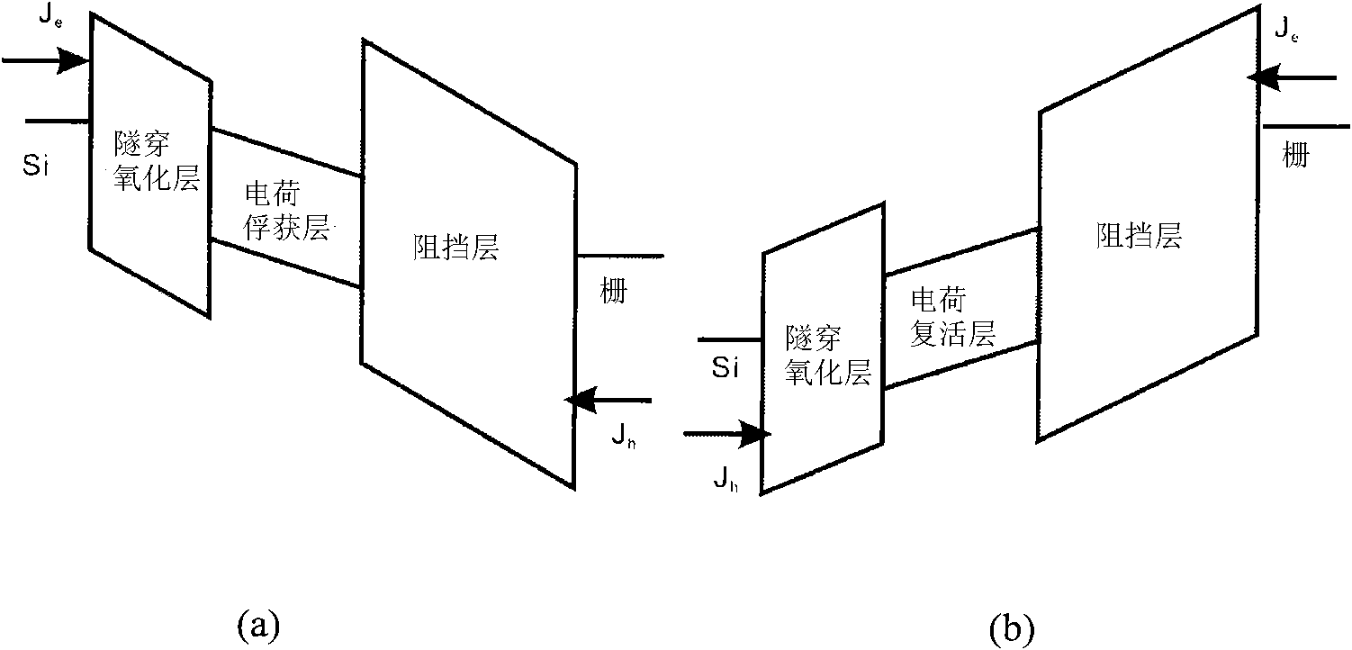
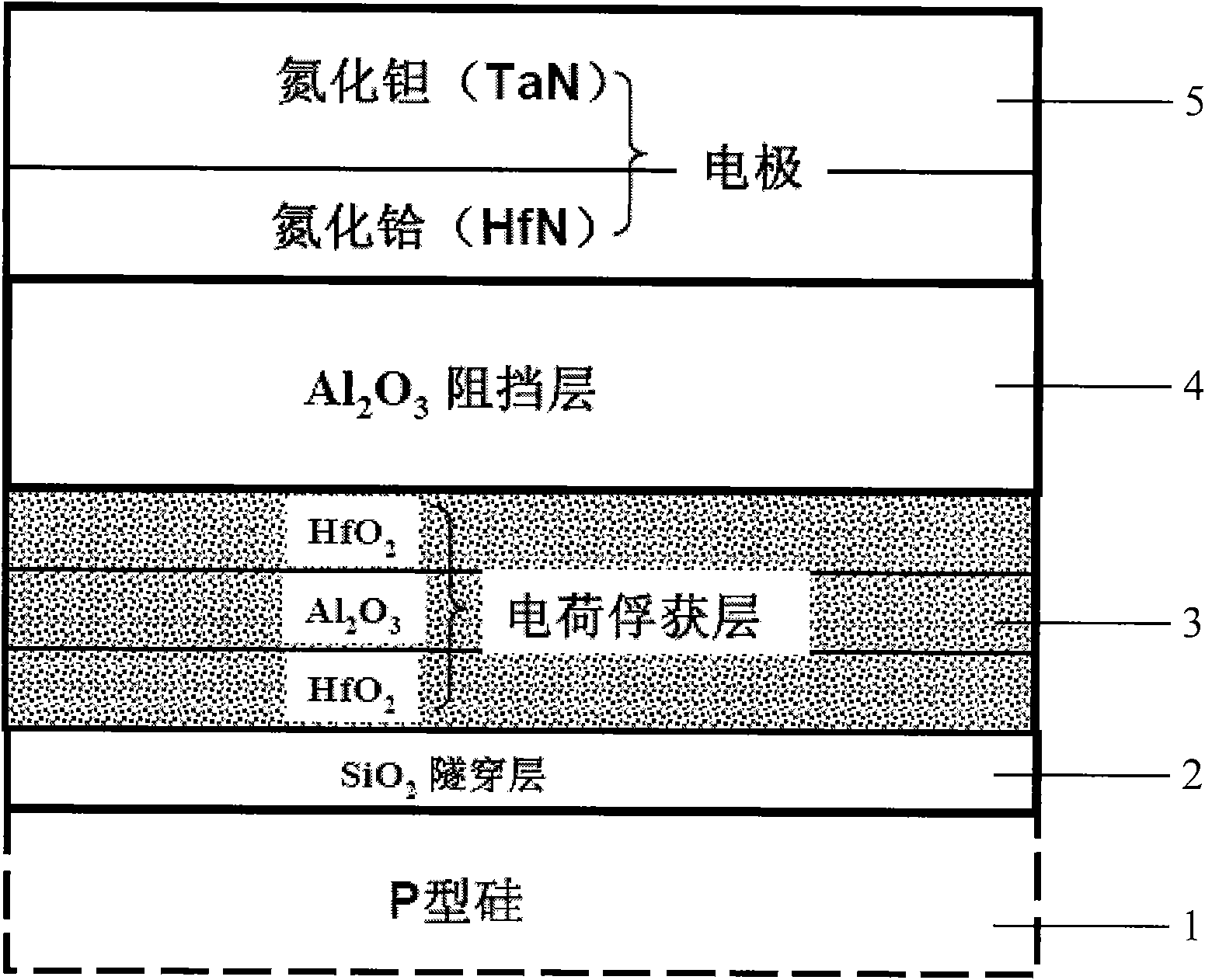
[0026] SiO is thermally oxidized in a dry oxygen atmosphere at 750-900°C 2 Make a charge tunneling layer with a physical thickness of 2-4 nanometers; then use atomic layer deposited HfO 2 / Al 2 o 3 / HfO 2 Sandwich nano-lamination as charge trapping layer, in which HfO 2 The physical thickness of the single layer is 1-3 nm, Al 2 o 3 The physical thickness of a single layer is 1-3 nanometers, and the physical thickness of the entire HAN layer is 3-9 nanometers; 2 o 3 As a barrier layer, its physical thickness is controlled at 6-12 nanometers, and high-temperature annealing after deposition is not required. Finally, the magnetron sputtered double-layer HfN / TaN is used as the metal electrode, in which HfN is directly connected with the charge blocking layer Al 2 o 3 touch.

[0027] The specific process steps are as follows:

[0028] (1) Perform standard RCA cleaning on the 4-8Ωcm ...


PUM

PropertyMeasurementUnit
Thicknessaaaaaaaaaa
Thicknessaaaaaaaaaa
Thicknessaaaaaaaaaa

Abstract

The invention relates to an erasable metal-insulator-silicon capacitor structure, belonging to the technical field of capacitors. The invention sequentially adopts an SiO2 film which is thermally oxidized by high-temperature dry oxygen as a charge tunneling layer, an HfO2 / Al2O3 / HfO2 sandwich nano lamination deposited by an atom layer as a charge capturing layer and an Al2O3 film deposited by the atom layer as a charge blocking layer; a substrate adopts P type monocrystal silicon; and a metal electrode adopts an HfN / TaN double-layer metal film prepared by a magnetron sputtering reaction, wherein the HfN directly contacts with the charge blocking layer Al2O3. The invention can effectively inhibit electron injected by the blocking layer in an erasure mode, enhance the storage property of thecapacitor obviously and enable the capacitor to have quick programming / erasure property, big storage window and high capacitance density, and has no erasure saturated phenomenon.

Description

technical field [0001] The invention belongs to the technical field of capacitors, in particular to a high-density rewritable metal-insulator-silicon capacitor structure. Background technique [0002] The growing market of portable electronic products has greatly stimulated the research and development of non-volatile memory. Among many non-volatile storage structures, flash memory is the best due to its excellent performance and good process compatibility 1 . In recent years, due to the continuous shrinking of memory cells, the next-generation flash memory based on silicon dioxide / silicon nitride / silicon dioxide (ONO) dielectric structure has received extensive attention and research 1-4 , because the polysilicon / ONO / silicon (SONOS) structure has lower cost and radiation resistance characteristics. In the usual SONOS structure, silicon nitride is used as the charge storage layer, and silicon dioxide is used as the blocking oxide layer. However, erase saturation and low c...

Claims


Application Information

Patent Timeline
IPC IPC(8): H01L29/94H01L21/02
Inventor 丁士进陈玮张敏张卫
Owner FUDAN UNIV
Why Eureka
Try Eureka