Micro solid-state laser module

A laser module and solid-state technology, which is applied to lasers, laser components, devices for controlling laser output parameters, etc., can solve problems such as low conversion efficiency

Inactive Publication Date: 2010-03-17
ALVIS TECH
View PDF5 Cites 4 Cited by
  • Summary
  • Abstract
  • Description
  • Claims
  • Application Information

AI Technical Summary

Problems solved by technology

[0006] Currently, wavelength converters commonly used in solid-state laser modules can be periodically poled lithium niobate crystals (Periodically Poled Lithium Niobate, PPLN for short), potassium vanadate crystals (KTiOPO 4 , referred to as KTP), LBO, BBO, ADP and other crystals, among them, PPLN has a higher wavelength conversion efficiency (up to about 50%); relatively, the conversion efficiency of KTP is much lower (about 5% to 10% %), but because the conversion efficiency of KTP is less sensitive to external temperature changes, and the component price is much lower than that of PPLN, so if KTP is used as the wavelength converter of the solid-state laser module, it will be very important for the low-priced market that does not require high performance. Competitiveness; KTP is a stacked (Bulk) type, its optical coupling aperture is larger, and it is easy to couple lasers; therefore, the present invention proposes a simplified micro-solid-state laser module architecture such as a micro-solid-state green laser module. And its package still adopts TO-can packaging (TO-can packaging) mode. Compared with traditional solid-state (green light) laser modules, it is expected to have overwhelming competitiveness in terms of module volume, performance, production capacity and price.

Method used


Image

  • Micro solid-state laser module
  • Micro solid-state laser module
  • Micro solid-state laser module

Examples


no. 1 example

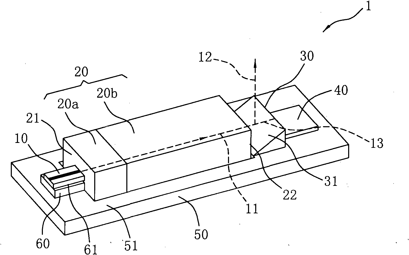
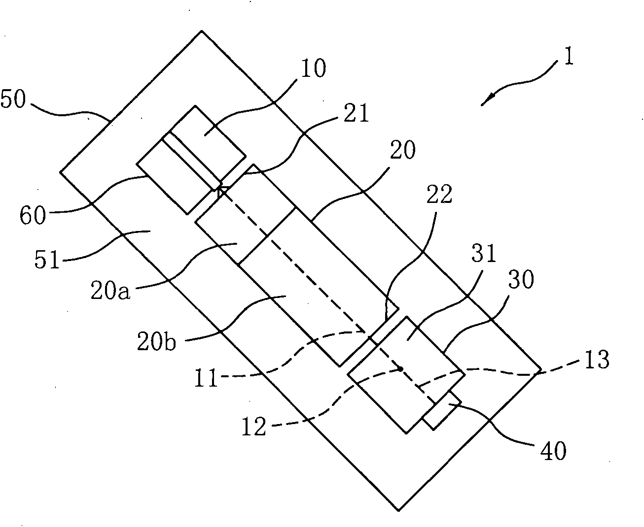
[0037] refer to figure 1 , 2 As shown, they are respectively a schematic diagram of the basic structure (which can be regarded as the first embodiment) of the miniature solid-state laser module of the present invention and a schematic top view thereof. The miniature solid-state laser module 1 of this embodiment adopts the mode of direct optical coupling, that is, this embodiment uses an 808 laser diode chip (808LD chip) to emit laser light with a wavelength of 808nm, and within a very short distance of about 2-3um, the incident In the nonlinear crystal 20a and the frequency doubling crystal 20b of the wavelength converter 20, it is emitted from the output end 22 of the wavelength converter 20 (frequency doubling crystal 20b), and passes through the spectroscopic device 30 with a 45-degree spectroscopic surface 31, so that the The first light beam 12 can be emitted in a direction 90 degrees from the original incident angle, that is, perpendicular to the installation plane 51 a...

no. 2 example

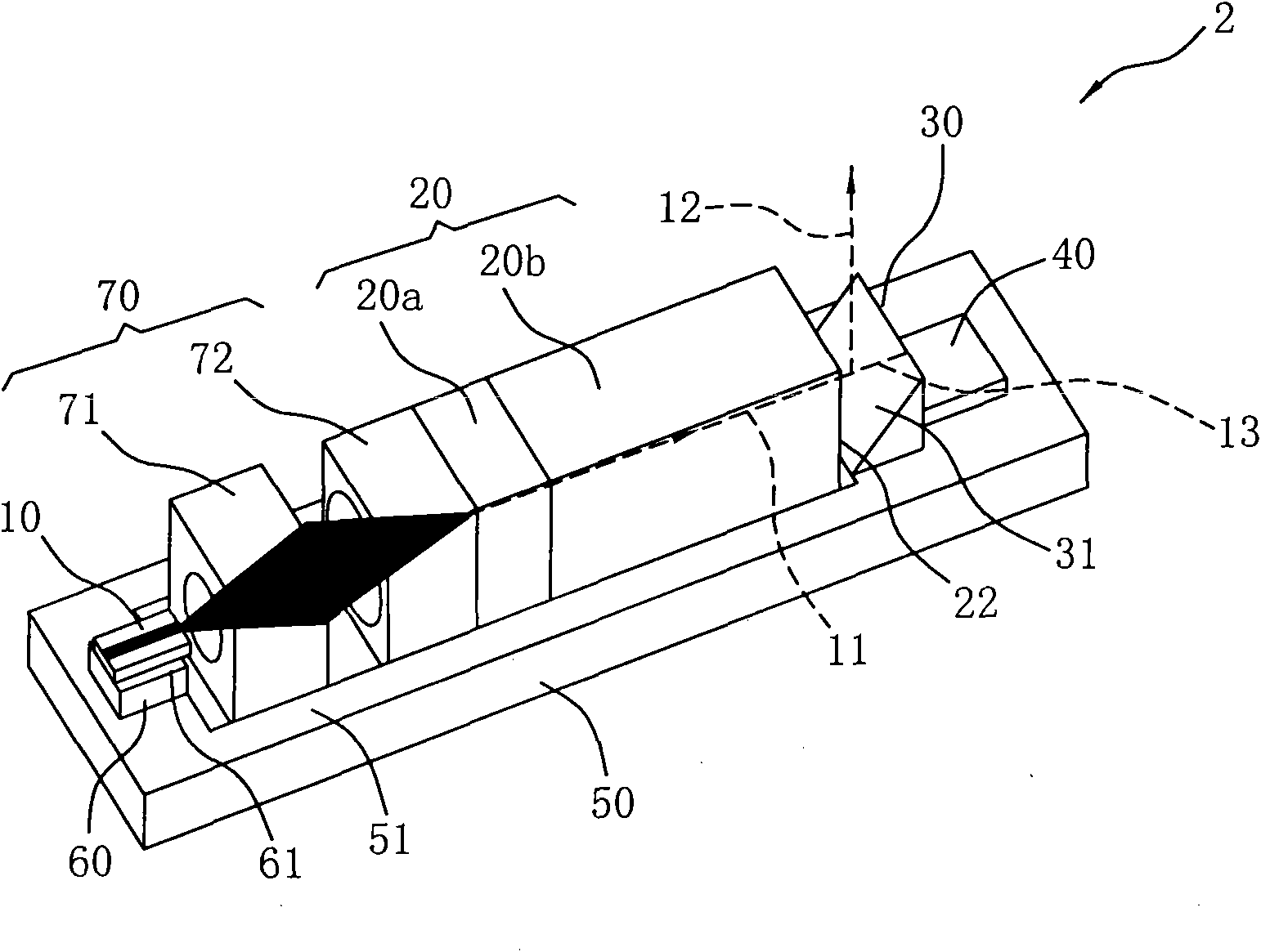
[0039] refer to image 3 As shown, it is a perspective view of the second embodiment of the micro solid-state laser module of the present invention. The miniature solid-state laser module 2 of this embodiment further adopts an indirect optical coupling method to replace the direct optical coupling method of the first embodiment, that is, an additional micro-optical element (Micro Optics) 70 is used to complete the indirect optical coupling requirement, The micro optics element (Micro Optics) 70 can be an optical coupling lens (coupling lens) (not shown), or as image 3 As shown, a collimator lens (collimator lens) 71 and a focusing lens (focusing lens) 72 are combined to form (that is, collimator lens + focusing lens), which not only greatly increases the tolerance of assembly positioning accuracy, but also facilitates Mass production, and the attenuation of light energy is also quite small (less than 2%), which will not affect the power of the light-transmitting laser.

no. 3 example

[0041] refer to Figure 4 , 5 , 6, which are respectively a reference diagram of the internal dimensions of a TO-Can packaging structure and two different schematic top views of the third embodiment of the micro solid-state laser module of the present invention. Due to the limited space for accommodating components in a TO-Can package structure, such as TO-5 Figure 4 As shown, the area of ​​its internal components that can be accommodated is about 5mm × 5mm, so if the solid-state laser 10 of the miniature solid-state laser module of the present invention and its base (Sub-mount) 60, wavelength converter are to be placed in such a limited area 20 such as nonlinear crystal 20a and frequency doubling crystal 20b (such as Nd:YAG and KTP), and other micro optics components (Micro Optics) 70 such as image 3 The shown collimator lens (collimator lens) 71 , focusing lens (focusing lens) and spectroscopic device 30 such as a prism and photodetector 40 and other components may have ...


PUM


Abstract

The invention discloses a micro solid-state laser module, which comprises the following main elements: a solid laser, a wavelength converter, a light splitting device and an optical detector, whereinthe solid laser is used for emitting the laser; the wavelength converter is used for converting the wavelength of the laser into lasers with different wavelengths, such as green light, according to afrequency doubling principle; the light splitting device, such as a prism, is arranged behind the wavelength converter and is used for splitting the lasers after the conversion into two light beams, namely the first light beam is that a main light beam contains most of the power and can vertically outward emit to become a main output light source, and the second light beam passes through the lightsplitting device, such as the prism, and enters the optical detector; the optical detector is used for detecting the optical power of the second light beam; the light splitting device is utilized toensure that all the elements can be packaged on one plane for treatment so as to be favourable for being packaged in a smaller TO-can package; and the compensating correction can also be performed bydirectly sensing the laser obtained after the conversion of the wavelength converter through the optical detector to ensure that the error of feedback compensation is minimum and is far superior to the conventional feedback mode.

Description

technical field [0001] The invention relates to a solid-state laser module, in particular to a miniature solid-state laser module. Background technique [0002] A solid state laser module is a common photoelectric device (Photo-electronic / Photonic Device), which uses a wavelength converter (wavelength conversion device, or wavelength conversion crystal) to convert a known wavelength to The laser light is converted into different wavelengths (λ 2 ) lasers, such as blue light, green light, etc., can be used according to different needs; therefore, photoelectric devices or laser modules are generally called wavelength conversion photonic devices (Wavelength Conversion Photonic Device). [0003] An optoelectronic device, such as the solid-state laser module referred to in this case, can choose to use wavelength converters with different structural designs, and basically each wavelength converter laser (wavelength λ 1 ) and converted laser (wavelength λ 2 ) between wavelength ...

Claims


Application Information

Patent Timeline
Patent Type & Authority Applications(China)
IPC IPC(8): H01S3/16H01S3/10H01S3/109H01S5/06
Inventor 陈致晓陈国仁温明华
Owner ALVIS TECH
Why Eureka
Try Eureka