Method for manufacturing field effect transistor

A field effect transistor and a manufacturing method technology are applied in the field of substrate thinning of gallium nitride-based microwave power field effect devices, and can solve the problem of poor consistency of brightness and finish on the back surface, and decreased stability and reliability of back metal metal. Problems such as the adhesion between the substrate and the back gold metal, to achieve the effect of high consistency, firm and stable adhesion, and uniform rate

Inactive Publication Date: 2010-06-02
SICHUAN LONGRUI MICROELECTRONICS
View PDF0 Cites 11 Cited by
  • Summary
  • Abstract
  • Description
  • Claims
  • Application Information

AI Technical Summary

Problems solved by technology

Usually, the use of physical and mechanical grinding will cause a thickness difference of about 10-20 μm on the 2-inch wafer, resulting in inconsistent thickness of the substrate, and poor consistency of backside brightness and smoothness.
Abrasives contain a lot of dust. For areas with poor brightness

Method used


Image

  • Method for manufacturing field effect transistor
  • Method for manufacturing field effect transistor
  • Method for manufacturing field effect transistor

Examples


Embodiment

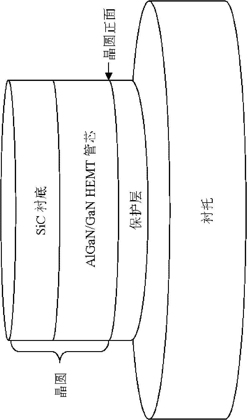
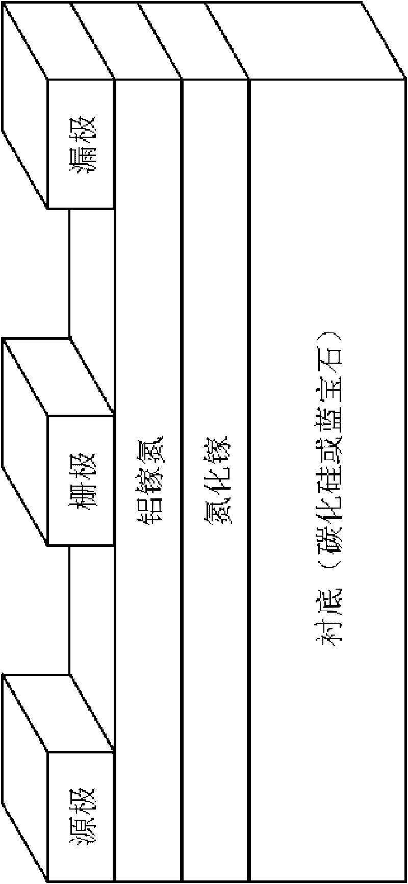
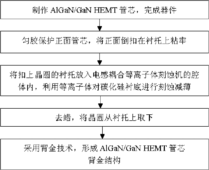
[0040] In this example, SF6 is used as the plasma gas source, and the silicon carbide substrate is etched by inductively coupled plasma etching to achieve thinning of the silicon carbide substrate. The etching method has the advantages of fast etching rate and high etching precision. There is no mechanical load on the wafer during the entire thinning process, which reduces the possibility of cracking or chipping the 2-inch wafer and ensures the stability and reliability of the thinning process. The thinning method of ICP etching improves the uniformity of the thinning rate of the silicon carbide substrate, enhances the thickness uniformity of the thinned substrate, does not have small dust attached to the substrate, improves the adhesion ability of the substrate surface, and enhances the thickness of the substrate. The adhesion of the gold structure to the silicon carbide substrate makes the adhesion between the back gold structure and the silicon carbide substrate stronger an...


PUM

PropertyMeasurementUnit
Thicknessaaaaaaaaaa

Abstract

The invention relates to a manufacturing technology of a field effect transistor, in particular to a method for thinning a substrate of a gallium nitride-based microwave field effect device. Aiming at the defects of a substrate thinning technology in the method for manufacturing the field effect transistor in the prior art, the invention discloses a method for manufacturing the field effect transistor, improves the substrate thinning technology of the field effect transistor so as to adapt to the thinning of a high-hardness substrate material, and improve the quality of a substrate process technology, the quality of the substrate and the overall performance of the device. By using the method for manufacturing the field effect transistor, in the manufacturing technology process of the field effect transistor, a carborundum substrate and other high-hardness substrates of the field effect transistor can be etched to be thinned by plasma. The invention can avoid the break of wafers and improve the quality of thinned substrates and is particularly suitable for a manufacturing technology of gallium nitride-based field effect transistor devices.

Description

technical field [0001] The invention relates to the fabrication technology of a field effect transistor, in particular to a method for thinning the substrate of a gallium nitride-based microwave power field effect device. Background technique [0002] Gallium nitride (GaN), as the third-generation wide-bandgap semiconductor material, has a large bandgap (3.4eV), a high breakdown voltage (3.3MV / cm), and a high two-dimensional electron gas concentration (>10 13 cm 2 ), high velocity of saturated electrons (2.8×10 7 cm / s) and other characteristics have received extensive attention internationally. At present, the high frequency, high voltage, high temperature and high power characteristics of AlGaN / GaN HEMT (Gallium Nitride-based High Electron Mobility Transistor) devices make them have great prospects in microwave power devices. [0003] In the semiconductor field effect transistor structure, the backside thinning process has an important impact on the performance of the...

Claims


Application Information

Patent Timeline
IPC IPC(8): H01L21/335H01L21/3065
Inventor 李滨李诚瞻刘新宇魏珂陈晓娟
Owner SICHUAN LONGRUI MICROELECTRONICS
Why Eureka
Try Eureka