Method for cleaning metal residue
A metal residue and wet cleaning technology, which is applied in the field of semiconductor manufacturing, can solve problems such as device reliability hazards, inability to completely remove Pt, and adverse effects on device electrical performance.
- Summary
- Abstract
- Description
- Claims
- Application Information
AI Technical Summary
Problems solved by technology
Method used
Image
Examples
Embodiment 1
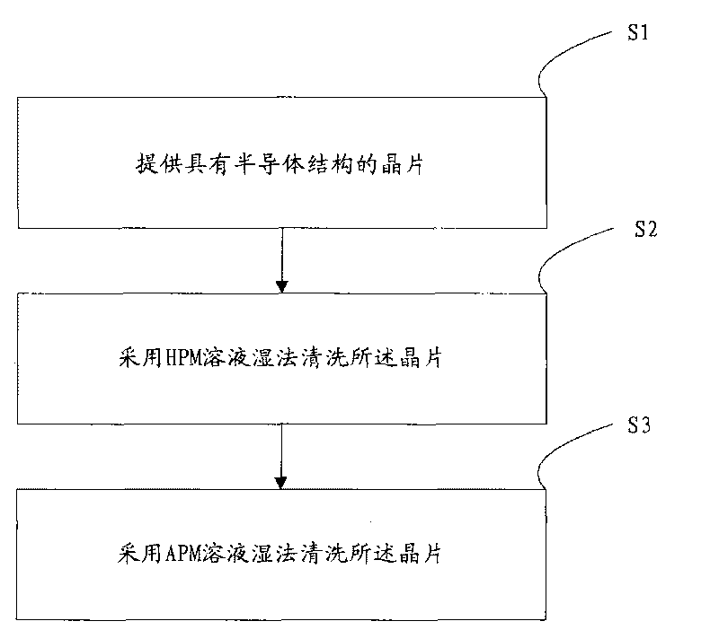
[0050] The preferred embodiment of the metal residue removal method will be described in detail with the background of the metal silicide fabrication process. figure 1 It is a flowchart of the removal method of the metal residue.
[0051] Step S1: providing a wafer with a semiconductor structure with Pt-containing metal residues on the semiconductor structure.
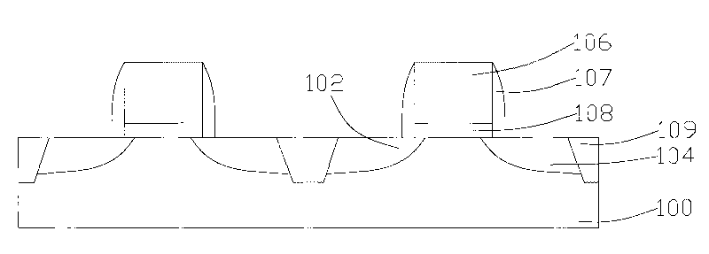
[0052] Specifically, such as figure 2 As shown, a substrate 100 is provided, and the substrate 100 may be a wafer of single crystal silicon. There is a semiconductor device in the substrate 100, for example, the semiconductor device is a metal oxide semiconductor (MOS) transistor, figure 2 Only two MOS transistors are shown in , and the two MOS transistors have shallow trench isolation (STI) 109 to isolate different semiconductor devices.
[0053] The MOS transistor includes a source 102 , a drain 104 and a gate 106 with a gate oxide layer 108 between the substrate 100 and the gate 106 . There is also a gate spac...
Embodiment 2
[0067] Figure 7 It is a flowchart of the method for removing metal residues described in this embodiment.
[0068] Referring to step A1 : providing a wafer having a semiconductor structure with Pt-containing metal residues thereon. This step A1 is the same as the step S1 of the first embodiment, for details, please refer to Figure 2 to Figure 5 , which will not be repeated here.
[0069] Refer to step A2: using SPM solution to wet clean the wafer with MOS transistors on the substrate 100 to remove the metal Ni in the metal residue 111 . Described SPM solution is sulfuric acid (H 2 SO 4 ) and hydrogen peroxide (H 2 o 2 ) mixed solution, its volume ratio concentration is H 2 SO 4 :H 2 o 2 =(3-5):1, during cleaning, the pre-configured SPM solution is atomized and sprayed onto the wafer surface, the temperature of the SPM solution is controlled in the range of 80°C to 99°C, for example, 85°C, 90°C , 95°C, within this temperature range, the SPM solution can fully react w...
Embodiment 3
[0077] Figure 8 It is a flowchart of the method for removing metal residues described in this embodiment.
[0078] Referring to step B1: providing a wafer having a semiconductor structure with Pt-containing metal residues thereon. This step B1 is the same as the step S1 of the first embodiment, for details, please refer to Figure 2 to Figure 5 , which will not be repeated here.
[0079] Referring to step B2: using the first SPM solution to wet-clean the substrate 100 to remove metal Ni in the metal residue 111 . The first SPM solution is sulfuric acid (H 2 SO 4 ) and hydrogen peroxide (H 2 o 2 ) mixed solution, its volume ratio concentration is H 2 SO 4 :H 2 o 2 =(3-5): 1, during cleaning, spray the pre-configured first SPM solution onto the wafer surface after atomization, the temperature of the first SPM solution is controlled in the range of 80°C to 99°C, for example, 85°C, 90°C, 95°C, within this temperature range, the first SPM solution can fully react with m...
PUM
| Property | Measurement | Unit |
|---|---|---|
| Thickness | aaaaa | aaaaa |
Abstract
Description
Claims
Application Information
 - R&D Engineer
- R&D Manager
- IP Professional
- Industry Leading Data Capabilities
- Powerful AI technology
- Patent DNA Extraction
Browse by: Latest US Patents, China's latest patents, Technical Efficacy Thesaurus, Application Domain, Technology Topic, Popular Technical Reports.
© 2024 PatSnap. All rights reserved.Legal|Privacy policy|Modern Slavery Act Transparency Statement|Sitemap|About US| Contact US: help@patsnap.com


