SOI wafer-based MEMS structure manufacturing and dicing method

A wafer and dicing technology, applied in the direction of microstructure technology, microstructure devices, processing microstructure devices, etc., can solve the problems of low yield, expensive equipment, high process risk, etc., and achieve high yield, low cost, high efficiency effect

Active Publication Date: 2010-06-16
JIANGSU FANHUA GLASS CO LTD +1
View PDF0 Cites 23 Cited by
  • Summary
  • Abstract
  • Description
  • Claims
  • Application Information

AI Technical Summary

Problems solved by technology

[0005] In order to overcome the disadvantages of high process risk, expensive equipment, and low yield in existing MEMS wafer scribing, the present invention proposes a method for synchronously completing structure f

Method used


Image

  • SOI wafer-based MEMS structure manufacturing and dicing method
  • SOI wafer-based MEMS structure manufacturing and dicing method
  • SOI wafer-based MEMS structure manufacturing and dicing method

Examples


Embodiment 1

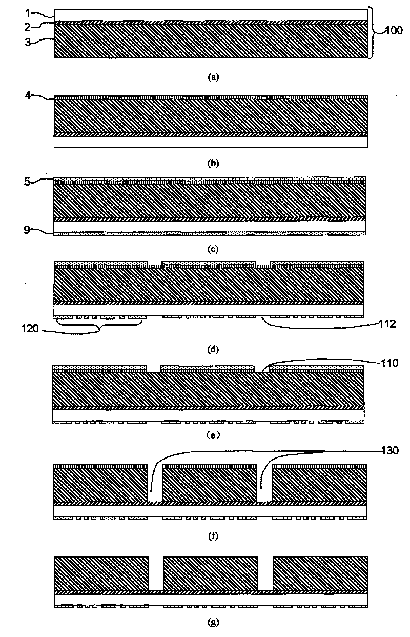
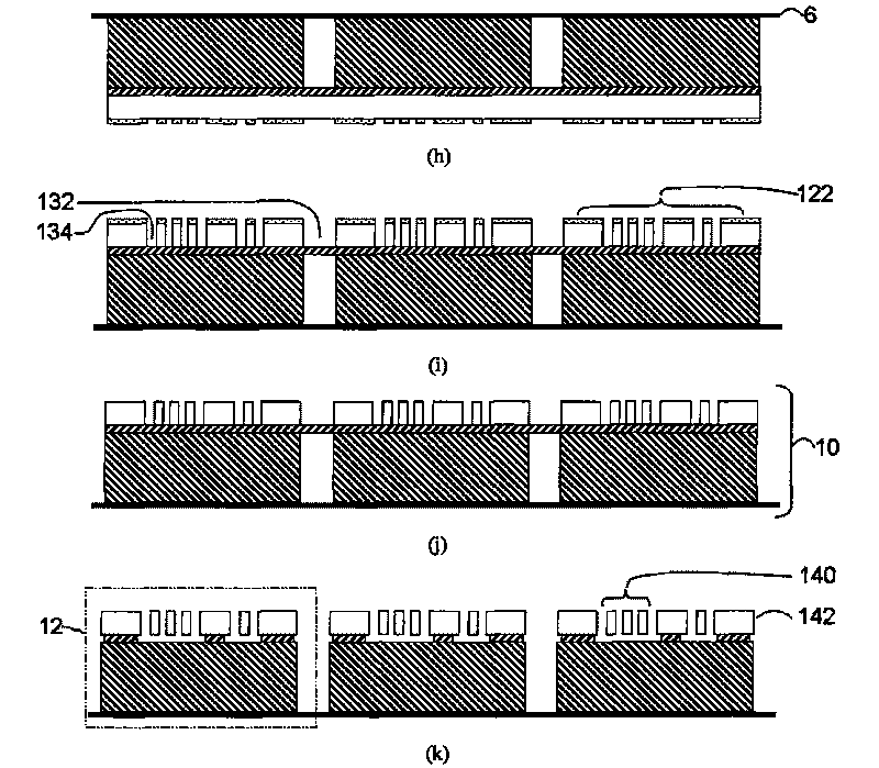
[0040] This embodiment is based on SOI wafer MEMS grating device structure fabrication and dicing method, refer to figure 1 (a)~(k), the structure of the grating device is referred to image 3 , the specific steps are:

[0041] Step 1: Refer to figure 1 (a), cleaning and pre-baking the SOI wafer 100 .

[0042] Step 2: Deposit a deep etch mask layer 4 with a thickness of 500 nm on the surface of the base layer 3. The deep etch mask layer 4 is made of metal aluminum, see figure 1 (b).

[0043] Step 3: Deposit a first photoresist layer 9 with a thickness of 1 μm on the surface of the top layer 1, deposit a second photoresist layer 5 with a thickness of 1 μm on the surface of the deep etching masking layer 4, and bake at a temperature of 110 degrees for 1 minute , see figure 1 (c).

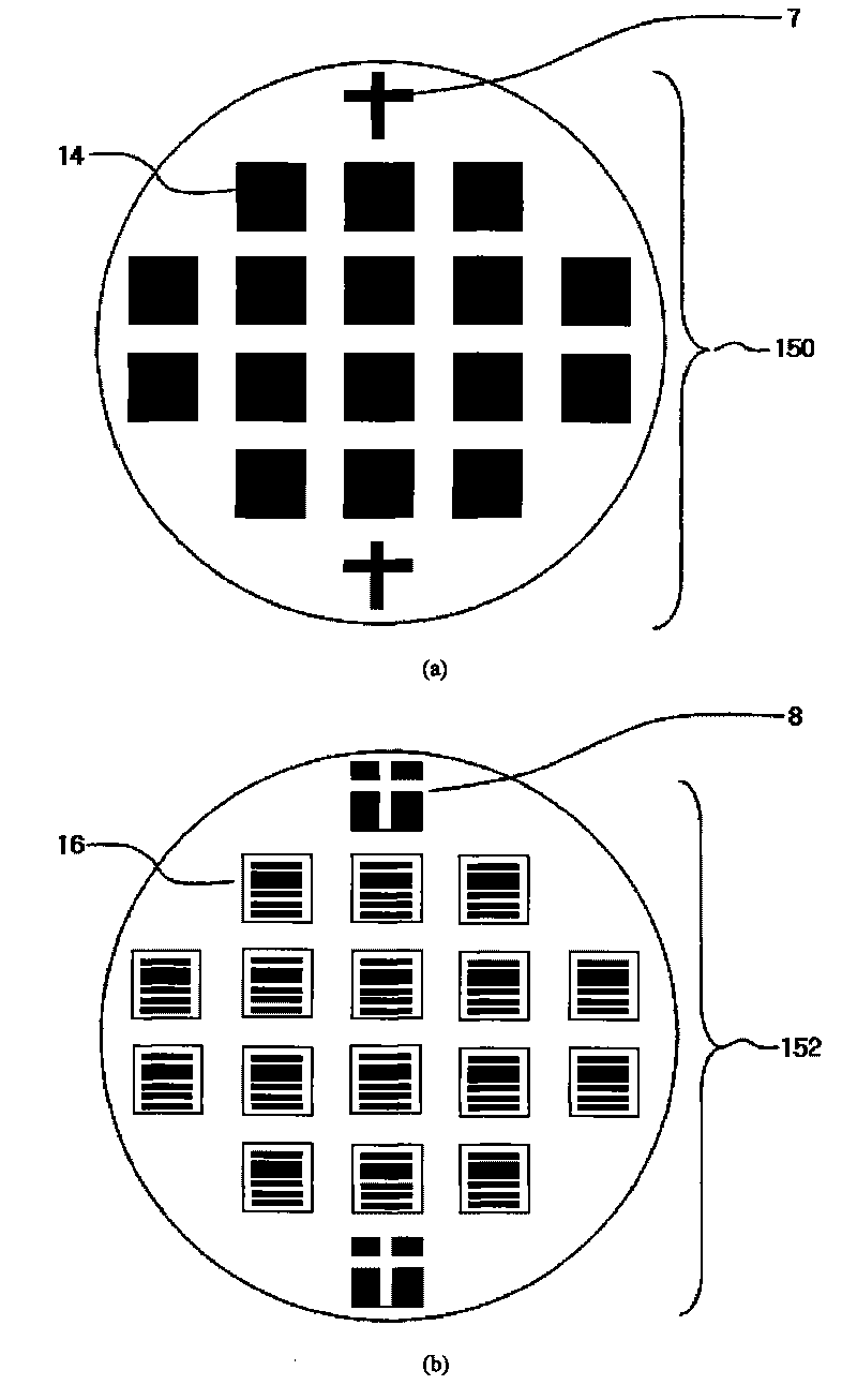
[0044] Step 4: Use the lower mask 150 and the upper mask 152 to perform double-sided photolithography on the wafer processed in step 3. The lower mask 150 and the upper mask 152 have the same ch...

Embodiment 2

[0053] This embodiment is based on SOI wafer MEMS gyroscope device structure fabrication and dicing method, refer to figure 1 (a)~(k), the structure of the gyroscope device is referred to Figure 4 , the specific steps are:

[0054] Step 1: For example figure 1 The SOI wafer 100 shown in (a) is cleaned and prebaked.

[0055] Step 2: Deposit a deep etch mask layer 4 with a thickness of 2 μm on the surface of the base layer 3. The deep etch mask layer 4 is made of silicon dioxide material, see figure 1 (b).

[0056] Step 3: Deposit a 0.9 μm thick first photoresist layer 9 on the surface of the top layer 1, deposit a 0.9 μm thick second photoresist layer 5 on the surface of the deep etching mask layer 4, and heat bake at a temperature of 90 degrees 1 minute, see figure 1 (c).

[0057] Step 4: Use the lower mask 150 and the upper mask 152 to perform double-sided photolithography on the wafer processed in step 3. The lower mask 150 and the upper mask 152 have the same chip un...


PUM


Abstract

The invention discloses an SOI wafer-based MEMS structure manufacturing and dicing method, which belongs to the field of the micromachining of a micro-electromechanical system and the dicing of a wafer. The method adopts key points that: the high aspect radio effect of ICP corrosion is utilized, and an MEMS structural mask and a mask corresponding to the MEMS structural mask are adopted to perform a conventional MEMS machining process on the front and back surfaces of the SOI wafer; and the machining process comprises glue spreading, photo-etching, corrosion, release and the like to synchronously finish manufacturing an MEMS structure and dicing the wafer. The SOI wafer-based MEMS structure manufacturing and dicing method has the advantages of (1) having no mechanical vibration, no stress damage, no heating, no shavings, no pollution and high rate of finished products, (2) not needing expensive dicing equipment, finishing manufacturing the MEMS structure and dicing the wafer on the basis of conventional MEMS process equipment and having low cost, (3) synchronously finishing the MEMS manufacturing process and the dicing process so as to obtain high efficiency, and (4) not needing to add a temporary or permanent protective layer, not influencing interaction between the equipment and external information, finishing the release at the same time of dicing and not damaging an MEMS movable structure in an intermediate process.

Description

technical field [0001] The invention relates to a method for synchronously completing MEMS structure fabrication and scribing based on SOI wafers, and belongs to the fields of microelectromechanical system micromachining and wafer slicing. Background technique [0002] The development of IC industry has greatly promoted the progress of dicing technology. The widely used scribing method is based on the grinding wheel grinding of diamond blades. This method has become the mainstream of wafer dicing due to its high efficiency, simple and controllable process and other advantages. With the development of micro-electro-mechanical systems, an emerging discipline, and the gradual acceleration of the industrialization process, the rotary grinding wheel scribing technology has gradually highlighted serious defects: grinding wheel grinding will produce mechanical vibration, and the pressure and torque between the grinding wheel and the silicon wafer will cause The internal stress of ...

Claims


Application Information

Patent Timeline
IPC IPC(8): B81C99/00B81C3/00
Inventor 李晓莹孙瑞康乔大勇燕斌虞益挺李太平
Owner JIANGSU FANHUA GLASS CO LTD
Why Eureka
Try Eureka