

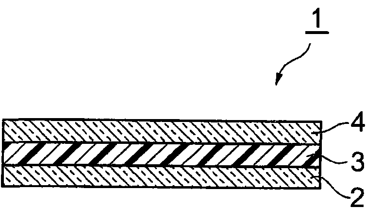
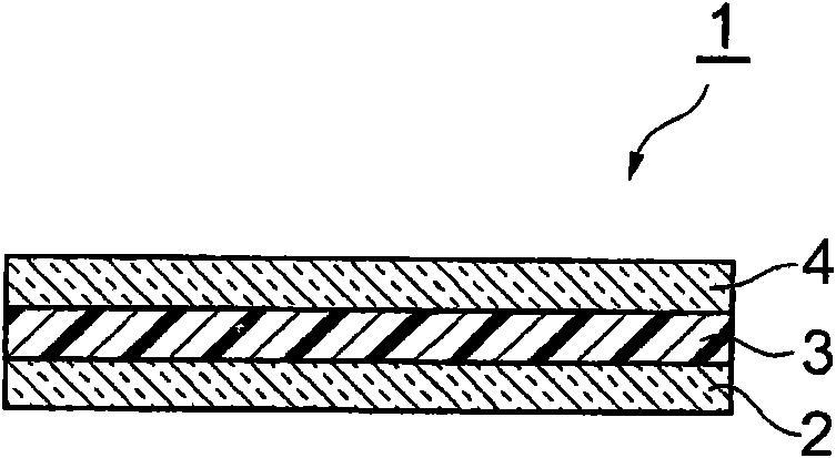
Light-sensitive resin composite and method for manufacturing printed circuit board using same
A technology of photosensitive resin and composition, applied in the field of photosensitive resin composition, can solve the problems of insufficient illumination of light source, low sensitivity of photosensitive resin composition and photosensitive element, poor production efficiency and the like
- Summary
- Abstract
- Description
- Claims
- Application Information
AI Technical Summary
Problems solved by technology
Method used
Image

Examples
Embodiment
[0096] Hereinafter, the present invention will be specifically described based on examples, but the present invention is not limited thereto.
[0097] The composition was compounded according to the compounding composition (unit: part by mass) shown in following Table 1 and 2, and the solution of the photosensitive resin composition of Examples 1-6 and Comparative Examples 1 and 2 was obtained.
[0098] [Table 1]
[0099]
[0100] [Table 2]
[0101]
[0102] In addition, each component in Tables 1-2 is as follows.
[0103] Bisphenol A skeleton EO modified dimethacrylate: manufactured by Hitachi Chemical Industry Co., Ltd. (Hitachi Chemical Industry Co., Ltd.), trade name "FA-321M";
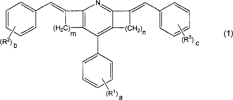
[0104] MAP-PDSP: 1,2,3,5,6,7-Hexahydro-8-phenyl-3,5-bis[(4-dimethylaminophenyl)methylene]-dicyclopentacene pyridine;
[0105] EAP-PDSP: 1,2,3,5,6,7-Hexahydro-8-phenyl-3,5-bis[(4-diethylaminophenyl)methylene]-dicyclopentacene pyridine;
[0106] 3-MOP-PDSP: 1,2,3,5,6,7-Hexahydro-8-phenyl...
Synthetic example 1
[0114] Add dimethylaminobenzaldehyde (1.49g, 10mmol), cyclopentanone (0.42g, 5mmol), ammonium acetate (3.85g, 50mmol) and ethanol (25mL) into the flask, and stir to obtain a uniform reaction solution. Next, 1 mL of 30% hydrogen peroxide aqueous solution was added to the above reaction solution, refluxed for 1 hour, and left to stand overnight to precipitate the crude crystals of MAP-PDSP. The crude crystals were filtered, washed with acetone, and then recrystallized with acetone to obtain MAP-PDSP. Maximum Absorption Wavelength (λ max ) is 440nm.
Synthetic example 2
[0116] EAP-PDSP was obtained in the same manner as in Synthesis Example 1, except that diethylaminobenzaldehyde (1.77 g, 10 mmol) was used instead of dimethylaminobenzaldehyde (1.49 g, 10 mmol). Maximum Absorption Wavelength (λ max ) is 440nm.
PUM
| Property | Measurement | Unit |
|---|---|---|
| wavelength | aaaaa | aaaaa |
| thickness | aaaaa | aaaaa |
Abstract
Description
Claims
Application Information