Method for preparing selective emission area of crystalline silicon solar cell

A solar cell, selective technology, applied in circuits, electrical components, semiconductor devices, etc., can solve problems such as large increase in equipment, screen printing pollution, and complex processes

Inactive Publication Date: 2010-06-16
浙江向日葵聚辉新能源科技有限公司
View PDF0 Cites 7 Cited by
  • Summary
  • Abstract
  • Description
  • Claims
  • Application Information

AI Technical Summary

Problems solved by technology

However, these methods are relatively complicated in process, require a large amount of equipment, and the relative cost will increase significantly. They are only suitable for small-scale experiments or small-scale production, and it is difficult to achieve mass production.
In recent years, there has been a method for preparing selective emission regions by screen printing phosphorous paste, but due to the pollution problem caused by screen printing, it has not been widely used in practice.

Method used


Image

  • Method for preparing selective emission area of crystalline silicon solar cell
  • Method for preparing selective emission area of crystalline silicon solar cell

Examples


Embodiment 1

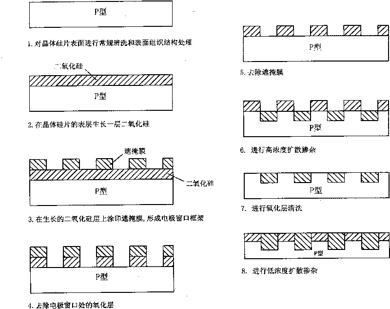
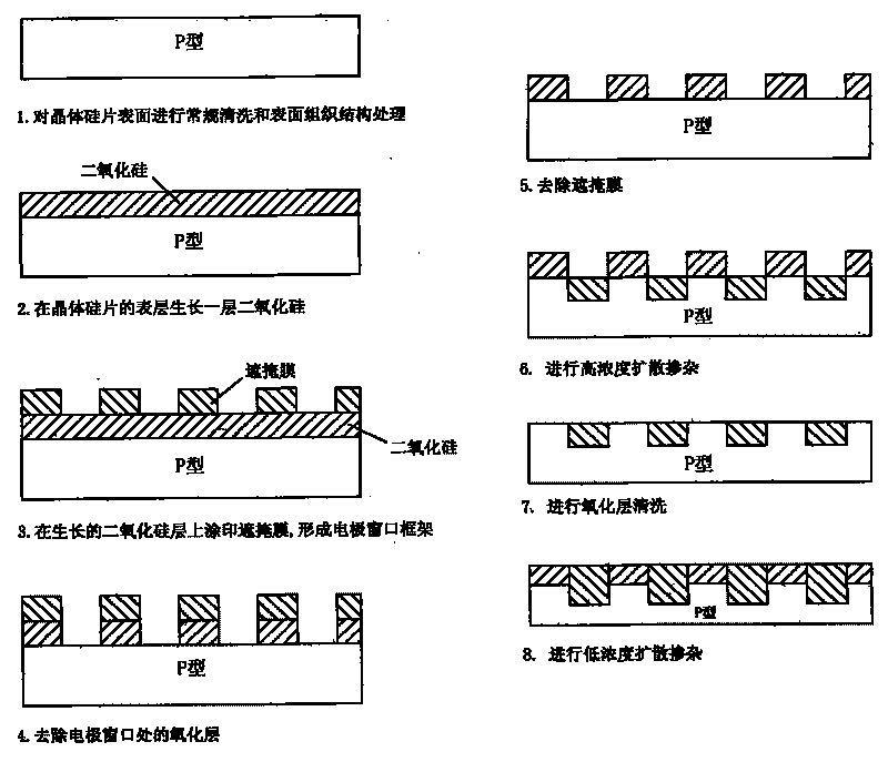
[0030] 1. Perform routine cleaning and surface structure treatment on the surface of crystalline silicon wafers.

[0031] 2. A layer of silicon dioxide is grown on the surface of the crystalline silicon wafer, and the thickness is controlled at 5nm.

[0032] 3. Applying a masking film on the grown silicon dioxide layer by screen printing to form an electrode window frame.

[0033] 4. Removing the oxide layer at the electrode window, that is, removing the silicon dioxide layer not covered by the masking film. A 10% hydrofluoric acid solution is selected to remove the silicon dioxide layer not covered by the masking film.

[0034] 5. Use 5% sodium hydroxide solution to remove the masking film.

[0035] 6. The liquid source of phosphorus oxychloride is converted into a gaseous state, and high-concentration diffusion doping is carried out at a high temperature of 870°C for 55 minutes.

[0036] 7. Cleaning the oxide layer, that is, removing the silicon dioxide layer originally c...

Embodiment 2

[0043] 1. Perform routine cleaning and surface structure treatment on the surface of crystalline silicon wafers.

[0044] 3. A layer of silicon dioxide is grown on the surface of the crystalline silicon wafer, and the thickness is controlled at 6nm.

[0045] 3. Applying a masking film on the grown silicon dioxide layer by screen printing to form an electrode window frame.

[0046] 4. Removing the oxide layer at the electrode window, that is, removing the silicon dioxide layer not covered by the masking film. A 12% hydrofluoric acid solution is selected to remove the silicon dioxide layer not covered by the masking film.

[0047] 5. Use 5% sodium hydroxide solution to remove the masking film.

[0048] 6. The phosphorus oxychloride liquid source is converted into a gaseous state, and high-concentration diffusion doping is carried out at a high temperature of 880°C for 53 minutes.

[0049] 7. Cleaning the oxide layer, that is, removing the silicon dioxide layer originally cove...

Embodiment 3

[0056] 1. Perform routine cleaning and surface structure treatment on the surface of crystalline silicon wafers.

[0057] 4. A layer of silicon dioxide is grown on the surface of the crystalline silicon wafer, and the thickness is controlled at 6.5nm.

[0058] 3. Applying a masking film on the grown silicon dioxide layer by screen printing to form an electrode window frame.

[0059] 4. Removing the oxide layer at the electrode window, that is, removing the silicon dioxide layer not covered by the masking film. A 15% hydrofluoric acid solution is selected to remove the silicon dioxide layer not covered by the masking film.

[0060] 5. Use 5% sodium hydroxide solution to remove the masking film.

[0061] 6. The phosphorus oxychloride liquid source is converted into a gaseous state, and high-concentration diffusion doping is carried out at a high temperature of 885°C for 50 minutes.

[0062] 7. Cleaning the oxide layer, that is, removing the silicon dioxide layer originally co...


PUM


Abstract

The invention relates to a method for preparing a selective emission area of a crystalline silicon solar cell. The method comprises the following steps of: (1) growing a layer of silicon dioxide on the surface of a crystalline silicon slice; (2)coating a masking film on the grown silicon dioxide layer to form a frame of an electrode window; (3) removing an oxide layer at the position of the electrode window, namely removing the silicon dioxide layer not covered by the masking film; (4) removing the masking film; (5) performing high-concentration diffusion doping; (6) washing the oxide layer, namely removing the silicon dioxide layer originally covered by the masking film; and (7) performing low-concentration diffusion doping. The method has the advantages of simple preparation process, low cost, no pollution and an average cell conversion efficiency of 18.5 percent.

Description

technical field [0001] The invention relates to a method for preparing a selective emission region of a crystalline silicon solar cell. Background technique [0002] As crystalline silicon solar cells occupy the market share, further improving conversion efficiency and reducing costs have become important issues for domestic and foreign crystalline silicon solar cell manufacturers to solve. In recent years, in the field of research, the laboratory efficiency of small-area monocrystalline silicon cells has reached 24.7%. However, the preparation process of these high-efficiency batteries is too complicated to meet the requirements of industrialization. There are many ways to realize the selective emission region, the most common ones are photolithography, laser grooving, and so on. However, these methods are relatively complex in process, require a large amount of equipment, and the relative cost will increase significantly. They are only suitable for small-scale experiment...

Claims


Application Information

Patent Timeline
Patent Type & Authority Applications(China)
IPC IPC(8): H01L31/18
CPCY02P70/50
Inventor 周晓兵赵明陈国其楼佳伟
Owner 浙江向日葵聚辉新能源科技有限公司
Why Eureka
Try Eureka