Organic electroluminescent device and preparation method thereof

An electroluminescent device, organic technology, applied in the direction of electric solid-state devices, chemical instruments and methods, semiconductor/solid-state device manufacturing, etc., can solve the problems of quenching the concentration of small molecule organic fluorescent dyes, changing the color of light emission, reducing the brightness of light emission, etc. , to achieve the effects of easy realization of large-area display, improvement of utilization rate, and avoidance of concentration quenching

Inactive Publication Date: 2011-07-27
UNIV OF ELECTRONICS SCI & TECH OF CHINA
View PDF0 Cites 0 Cited by
  • Summary
  • Abstract
  • Description
  • Claims
  • Application Information

AI Technical Summary

Problems solved by technology

Generally, it is doped in a host material with higher exciton energy to realize the luminescence of dye molecules, but small molecule organic fluorescent dyes have problems such as concentration quenching at high concentrations.
As time goes by, the fluorescent material is prone to phase separation from the matrix molecules, resulting in inhomogeneity of doping, affecting device performance, reducing luminous brightness, efficiency, and changing luminous color, etc.

Method used


Image

  • Organic electroluminescent device and preparation method thereof
  • Organic electroluminescent device and preparation method thereof
  • Organic electroluminescent device and preparation method thereof

Examples


Embodiment 1

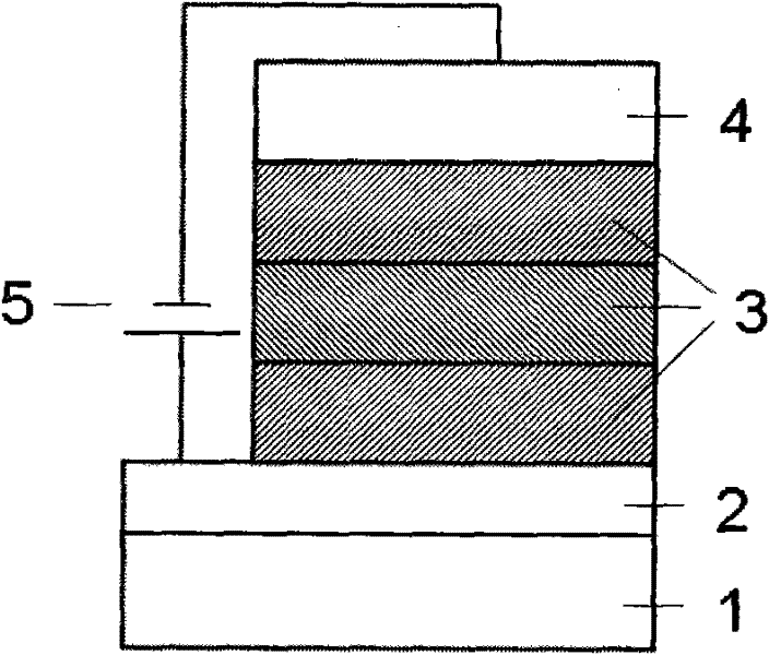
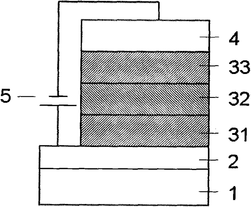
[0093] Such as figure 2 As shown, the organic functional layer 3 in the structure of the device includes a hole transport layer 31 , a light emitting layer 32 , and an electron transport layer 33 .

[0094] The hole transport layer material of the device is NPB, the light emitting layer material is material 1, and the electron transport material is Alq 3 , The cathode layer is made of Mg:Ag alloy. The entire device structure is described as:

[0095] Glass substrate / ITO / NPB(50nm) / Material 1(10nm) / Alq 3 (30nm) / Mg:Ag(100nm)

[0096] The preparation method is as follows:

[0097] ①Use ethanol solution, acetone solution and deionized water to ultrasonically clean the transparent conductive substrate ITO glass, and dry it with dry nitrogen after cleaning. Wherein the ITO film on the glass substrate is used as the anode layer of the device, the square resistance of the ITO film is 10Ω / □, and the film thickness is 180nm.

[0098] ②The dried substrate was moved into a vacuum ch...

Embodiment 2

[0105] Such as figure 2 As shown, the organic functional layer 3 in the structure of the device includes a hole transport layer 31 , a light emitting layer 32 , and an electron transport layer 33 .

[0106] The hole transport layer material of the device is NPB, the light emitting layer material is material 2, the electron transport material is TPBI, and the cathode layer uses Mg:Ag alloy. The entire device structure is described as:

[0107] Glass substrate / ITO / NPB(50nm) / Material 2(10nm) / TPBI(30nm) / Mg:Ag(100nm)

[0108] The fabrication process of the device is similar to that of Example 1.

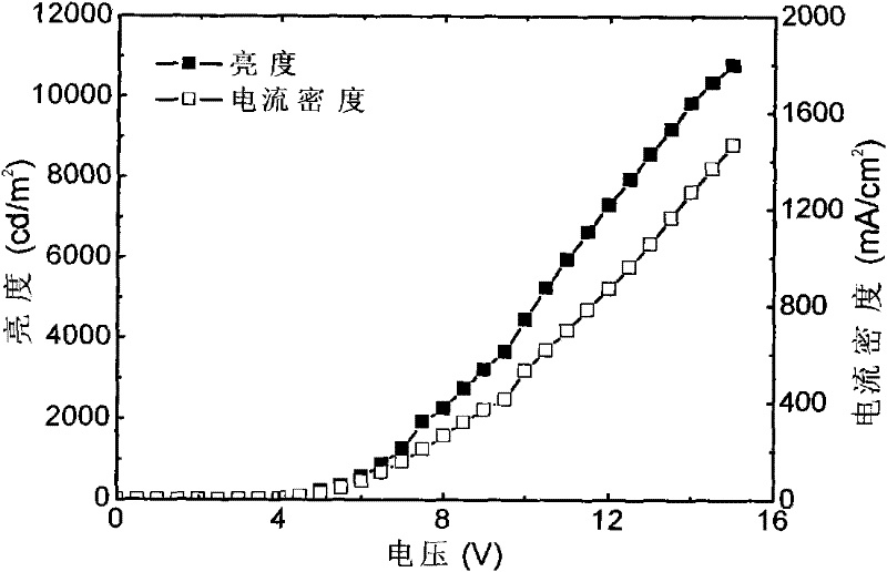
[0109] For the current-voltage-brightness characteristic curve of the device and the luminescence spectrum curve of the device, please refer to the attached Figure 5 and 6 .

Embodiment 3

[0111] Such as Figure 7 As shown, the organic functional layer 3 in the structure of the device includes a light-emitting layer that doubles as a hole transport layer 34 and an electron transport layer 33 .

[0112] The light-emitting layer of the device doubles as the hole transport layer is a doping system of material 3 and PVK, and the electron transport material is Alq 3 , The cathode layer is made of Mg:Ag alloy. The entire device structure is described as:

[0113] Glass substrate / ITO / PVK: Material 3 / Alq 3 (30nm) / Mg:Ag(100nm)

[0114] The preparation method is as follows:

[0115] ①Use ethanol solution, acetone solution and deionized water to ultrasonically clean the transparent conductive substrate ITO glass, and dry it with dry nitrogen after cleaning. Wherein the ITO film on the glass substrate is used as the anode layer of the device, the square resistance of the ITO film is 10Ω / □, and the film thickness is 180nm.

[0116] ②The dried substrate was moved into a...


PUM

PropertyMeasurementUnit
thicknessaaaaaaaaaa
thicknessaaaaaaaaaa

Abstract

The invention discloses an organic electroluminescent device, comprising a substrate, an anode layer and a cathode layer, wherein the anode layer or the cathode layer is positioned on the surface of the substrate. The organic electroluminescent device also comprises organic functional layers between the anode layer and the cathode layer. The organic functional layers at least include a luminescent layer which emits light by being driven by an applied power source. The luminescent material combines the organic fluorescent dye with the matrix molecules by chemical bonds by way of chemical crosslinking, so that energy transfer of the luminescent material is improved, thus not only avoiding the complex process caused by doping, but also avoiding the dye from being separated in the matrix molecules, optimizing the device structure and improving the luminescent efficiency, brightness and stability of the device.

Description

technical field [0001] The invention relates to the technical field of organic photoelectric devices in electronic components, and relates to an organic electroluminescent device based on fluorescent materials and a preparation method thereof. Background technique [0002] With the footsteps of human society entering the 21st century, the optoelectronic technology industry has developed vigorously, and people have higher and higher performance requirements for the carrier of the human-machine interface-information display devices. In recent years, due to the widespread use of liquid crystal displays (LCDs) and plasma displays (PDPs), the flat panel display industry has achieved tremendous development. Among them, organic electroluminescent displays (OLEDs) have a series of advantages such as self-luminescence, low-voltage DC drive, high and low temperature resistance, full curing, wide viewing angles, and rich colors. Compared with liquid crystal displays, organic electrolum...

Claims


Application Information

Patent Timeline
Patent Type & Authority Patents(China)
IPC IPC(8): H01L51/50H01L51/54H01L51/56C09K11/06
Inventor 于军胜王娜娜周立敏蒋亚东
Owner UNIV OF ELECTRONICS SCI & TECH OF CHINA
Why Eureka
Try Eureka