NPN (negative-positive-negative) heterojunction bipolar-junction transistor laser

A transistor laser, heterojunction bipolar technology, applied in the direction of semiconductor lasers, lasers, laser components, etc., can solve the problems of material quality degradation in the active area, deterioration of device luminous performance, etc., to improve electrical performance and increase luminescence Performance, the effect of reducing the concentration

Inactive Publication Date: 2010-06-23
INST OF SEMICONDUCTORS - CHINESE ACAD OF SCI
View PDF0 Cites 14 Cited by
  • Summary
  • Abstract
  • Description
  • Claims
  • Application Information

AI Technical Summary

Problems solved by technology

[0003] In the reported transistor laser structure, the quantum well active region is placed in the base region. For NPN devices, this structure has an obvious disadvantage: when using Zn, which can linearly control the hole concentration, as the p-type dopant When impurity is mixed, Zn is easy to diffuse into the active region from the upper and lower directions, resulting in a significant decline in the quality of the material in the active region and deteriorating the luminous performance of the device [J.Appl.Phys., Vol 103, P.114505(2008)]

Method used


Image

  • NPN (negative-positive-negative) heterojunction bipolar-junction transistor laser
  • NPN (negative-positive-negative) heterojunction bipolar-junction transistor laser

Examples


no. 1 example

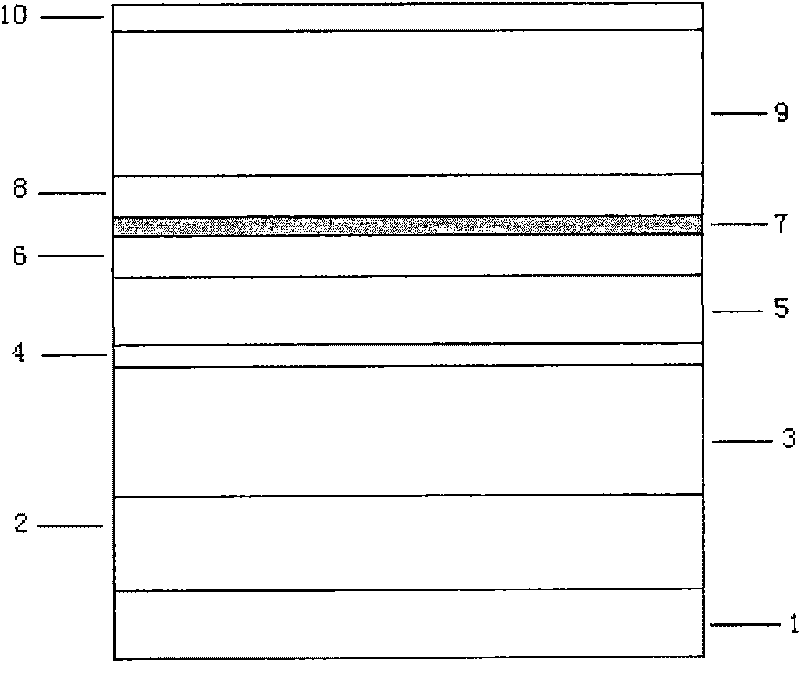
[0044] This embodiment is a specific process method for growing a GaAs-based NPN heterojunction bipolar transistor laser, which specifically includes the following steps:

[0045] 1) growing a gallium arsenide buffer layer 2 with a thickness of about 500 nm on the washed gallium arsenide substrate 1;

[0046] 2) growing InGaP (InGaP) with a thickness of 0.4 to 1.2 microns on the GaAs buffer layer 2 0.49 Ga 0.51 P) or aluminum gallium arsenide (Al x Ga 1-x As (0

[0047] 3) growing an n layer with a thickness of 30-70 nm on the lower cladding layer 3 + GaAs sub-collector layer 4;

[0048] 4) growing an i-type or weakly n-type doped gallium arsenic collector layer 5 with a thickness of 60-200 nm on the sub-collector layer 4;

[0049] 5) On the gallium arsenic collector layer 5, p + GaAs base layer 6;

[0050] 6) Growing an i-type InGaAs / GaAs quantum well active region 7 on the GaAs base layer ...

no. 2 example

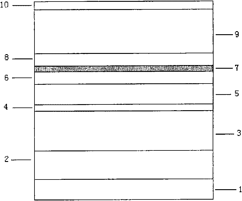
[0055] This embodiment is a specific process method for growing an indium phosphorus-based NPN heterojunction bipolar transistor laser, which specifically includes the following steps:

[0056] 1) growing an indium phosphorus buffer layer 2 with a thickness of about 500 nm on the washed indium phosphorus substrate 1;

[0057] 2) growing an indium phosphorus lower cladding layer 3 with a thickness of 0.4 to 1.2 microns on the indium phosphorus buffer layer 2 to confine the optical field and the electric field;

[0058] 3) On the indium phosphorus lower cladding layer 3, grow n + InP sub-collector layer 4;

[0059] 4) growing an i-type or weakly n-type doped indium phosphorus collector layer 5 with a thickness of 60-200 nm on the sub-collector layer 4;

[0060] 5) On the indium phosphorus collector layer 5, p + InGaAsP or InGaAs base layer 6;

[0061] 6) On the indium phosphorus base layer 6, grow the i-type indium gallium arsenide phosphorus quantum well active region layer...


PUM


Abstract

The invention relates to the technical field of semiconductor lasers, and discloses an NPN (negative-positive-negative) heterojunction bipolar-junction transistor laser which comprises a substrate (1), a buffer layer (2), a lower cladding layer (3), a sub-collector layer (4), a collector layer (5), a base layer (6), a quantum well active region layer (7), an emitter layer (8), an upper cladding layer (9) and a contact layer (10), wherein the quantum well active region layer is positioned between the base layer and the emitter layer, which reduces the dispersion of impurity Zn doped in the base layer to an active region on the one hand and decreases the dispersion of the impurity Zn doped in the base layer to the emitter layer on the other hand, thereby being beneficial to improving the optical and the electrical properties of elements. One part of electrons injected from an emitter illuminates in a radiative recombination way in the quantum well active region layer and the other part is collected by the collector layer to form a collector current.

Description

technical field [0001] The invention relates to the field of semiconductor optoelectronic devices, in particular to an NPN heterojunction bipolar transistor laser. Background technique [0002] In 2005, a research team from the University of Illinois in the United States first reported a semiconductor device called a heterojunction bipolar transistor laser in the world [Appl.Phys.Lett.Vol.87, P.131103 (2005) .], only using a relatively simple epitaxy and manufacturing process, the device simultaneously realizes the light emitting function of the laser and the amplification function of the transistor. The difference from ordinary transistors is that a quantum well is introduced in the base region of the transistor. Under a certain base-collector voltage, electrons will be injected into the base region from the collector region, and recombine with holes in the quantum well region to emit light. The light wave is reflected back and forth between the front and rear two cleavag...

Claims


Application Information

Patent Timeline
Patent Type & Authority Applications(China)
IPC IPC(8): H01S5/34H01S5/343
Inventor 梁松朱洪亮王圩
Owner INST OF SEMICONDUCTORS - CHINESE ACAD OF SCI
Why Eureka
Try Eureka