Manufacturing method of aluminum-substrate printed circuit board in-hole metallization

A technology for printed circuit boards and manufacturing methods, which is applied in the direction of electrical connection formation of printed components, can solve the problems of large pollution, inability to ensure thermal conductivity in holes, complex potassium dichromate treatment process, etc., and achieve high power consumption and convenience The effect of large-scale industrial production and good thermal conductivity

Inactive Publication Date: 2010-06-30
GCI SCI & TECH
View PDF0 Cites 3 Cited by
  • Summary
  • Abstract
  • Description
  • Claims
  • Application Information

AI Technical Summary

Problems solved by technology

[0003] In the aluminum-based copper-clad laminate and printed circuit board industry, the most commonly used methods of processing aluminum are potassium dichromate treatment and micro-arc oxidation treatment. Potassium dichromate treatment process is complicated and pollutes a lot; The oxidation treatment method isolates the aluminum base by generating alumina, which cannot guarantee the thermal conductivity in the hole, so the above two methods cannot be well applied to the metallization production of aluminum base printed circuit board holes

Method used


Image

  • Manufacturing method of aluminum-substrate printed circuit board in-hole metallization
  • Manufacturing method of aluminum-substrate printed circuit board in-hole metallization
  • Manufacturing method of aluminum-substrate printed circuit board in-hole metallization

Examples


Embodiment Construction

[0018] The present invention will be further described in detail below in conjunction with the accompanying drawings.

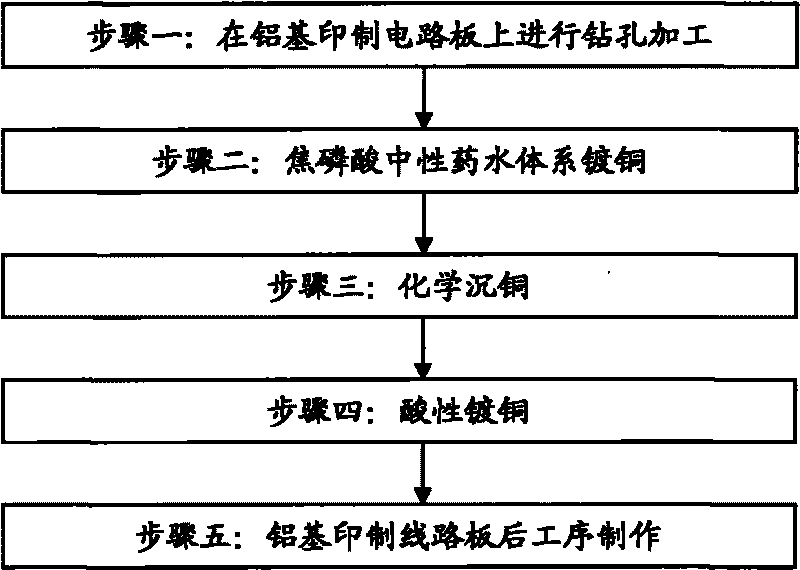
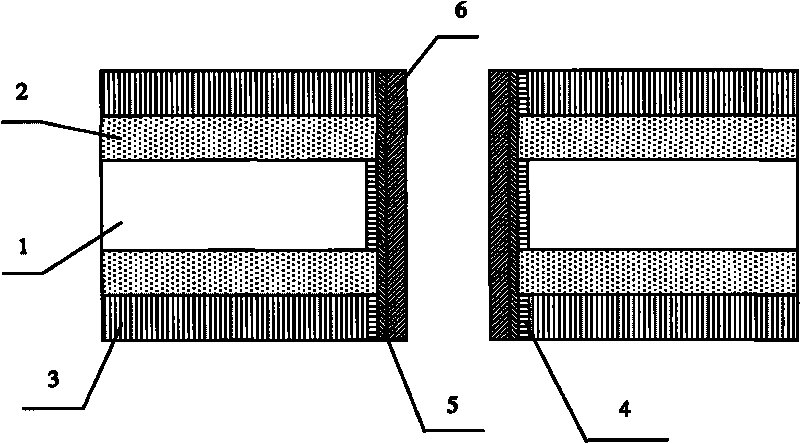
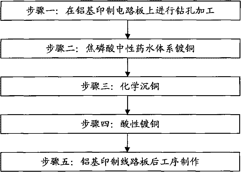
[0019] Such as figure 1 and figure 2 As shown, the present invention electroplates a layer of dense copper protective layer on the surface of the aluminum base through the pyrophosphoric acid neutral copper plating system after the drilling process, which effectively isolates the aluminum base from the strong acid-base potion in the electroless copper plating and acid copper plating process. The contact, so as to realize the metallization in the hole of the aluminum substrate. The aluminum-based printed circuit board includes an aluminum base layer 1 and an insulating dielectric layer 2 and a copper layer 3 sequentially arranged on both surfaces thereof, and the specific steps are as follows:

[0020] Step 1: Carry out drilling processing on the aluminum-based printed circuit board; this step is to carry out the drilling process on the aluminum-based coppe...


PUM


Abstract

The invention relates to a manufacturing method of aluminum-substrate printed circuit board in-hole metallization, which comprises the following steps: 1, drilling holes on an aluminum-substrate printed circuit board; 2, placing the aluminum-substrate printed circuit board in a neutral medicinal liquid system of pyrophosphoric acid to plate copper, namely, to form a layer of copper protective layer on an aluminum substrate; 3, performing electroless copper deposition to form a copper layer at non-metal positions; 4, performing acidic copper plating; and 5, performing post aluminum-substrate printed circuit board manufacturing process. In the invention, the aluminum substrate is effectively prevented from contacting medium-strong acidic and alkaline medicinal liquid in the processes of electroless copper deposition and acidic copper plating, which ensures the smooth operation of the subsequent processing steps of the aluminum-substrate printed circuit board. The process guarantees the welding reliability and high heat conductivity of the product after subsequent surface mounting, sets a high-concentration and high-power consumption trend for the development of the design of circuit boards, greatly reduces crosstalk between signals, reduces electric noises and further optimizes signal transmission. The method has a simple process and low cost and makes large-scale industrial production convenient.

Description

technical field [0001] The invention relates to a method for manufacturing a printed circuit board (PCB), in particular to a method for manufacturing metallization in holes of an aluminum-based printed circuit board. Background technique [0002] With the continuous development of electronic technology, the requirements for power dissipation and inductance of printed circuit boards are getting higher and higher. For example, high-speed and high-power microprocessors, ASICs, and signal processors generally require a power dissipation of 2 to 10kw, and the common printed circuit board structure has gradually been unable to meet the demand. Under this market demand, metallized substrates emerged as the times require. Through the high thermal conductivity of metal substrates, the design of printed boards has broken through the previous limitations, and has a higher assembly density, higher integration, and greater power consumption. direction development. At present, aluminum-...

Claims


Application Information

Patent Timeline
Patent Type & Authority Applications(China)
IPC IPC(8): H05K3/42
Inventor 任代学王晓伟
Owner GCI SCI & TECH
Why Eureka
Try Eureka