Group iii nitride semiconductor epitaxial substrate

A nitride semiconductor and epitaxial substrate technology, applied in semiconductor devices, semiconductor/solid-state device manufacturing, from chemically reactive gases, etc., can solve problems such as insufficient crystal quality and difficult crystal growth, and achieve improved crystal quality. The effect of suppressing cracks

Inactive Publication Date: 2010-07-14
SHOWA DENKO KK
View PDF1 Cites 13 Cited by
  • Summary
  • Abstract
  • Description
  • Claims
  • Application Information

AI Technical Summary

Problems solved by technology

However, AlGaN substrate Al x Ga 1-x The crystal quality of N(0
Especially Al with a high mole fraction of AlN x Ga 1-x N (0

Method used


Image

  • Group iii nitride semiconductor epitaxial substrate
  • Group iii nitride semiconductor epitaxial substrate
  • Group iii nitride semiconductor epitaxial substrate

Examples


Embodiment 1

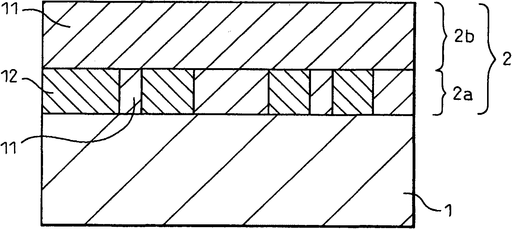
[0066] figure 1 It is a diagram schematically showing a cross-sectional structure of a Group III nitride semiconductor epitaxial substrate of the present invention in which AlN is laminated on a sapphire substrate produced in this example. In the figure, 1 is the substrate. 2 is Al x Ga 1-x The N (0≤x≤1) layer is composed of a layer 2a in which -C polar crystals and +C polar crystals are mixed, and a layer 2b in which only +C polar crystals exist. 11 is a +C polar crystal, and 12 is a -C polar crystal.

[0067] A structure in which AlN is laminated on a sapphire substrate is formed by the following procedure using a general reduced-pressure MOVPE device. First, a Φ2-inch (0001) sapphire substrate is loaded on a molybdenum suscepter. This was installed in a water-cooled reaction furnace using stainless steel through a load-lock chamber, and the furnace was cleaned by flowing nitrogen gas.

[0068] After changing the flowing gas in the vapor phase growth reaction furnace t...

Embodiment 2

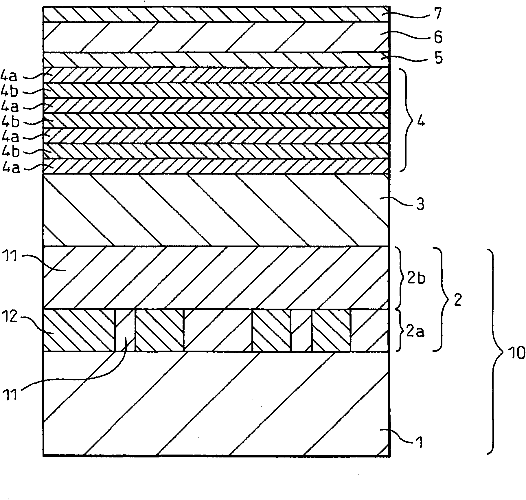
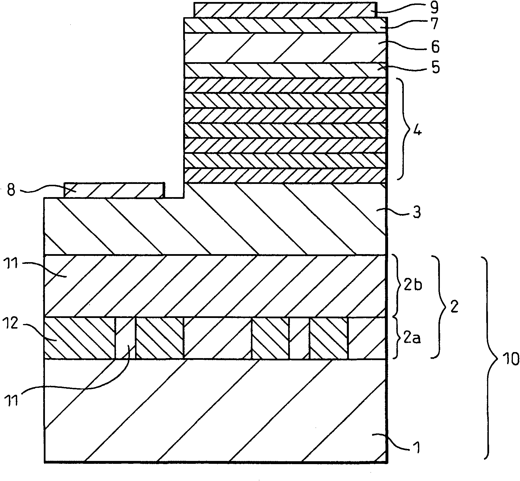
[0077] Fabricated on the Group III nitride epitaxial substrate of the present invention produced in Example 1 figure 2 A semiconductor stacked structure showing a cross-sectional structure in . In the figure, 1 and 2 with figure 1 Again, 1 is the base material, 2 is Al x Ga 1-x The N (0≤x≤1) layer is composed of a layer 2a in which -C polar crystals and +C polar crystals are mixed, and a layer 2b in which only +C polar crystals exist. 11 is +C polar crystal, 12 is -C polar crystal, 3 is Al 0.25 Ga 0.75 N(Si)n-capping layer, 4 is the MQW active layer, made of Al 0.12 Ga 0.88 N barrier layer 4a and Al 0.04 Ga 0.96 N well layer 4b. 5 is Al 0.35 Ga 0.65 N(Mg)p-electron blocking layer, 6 is Al 0.25 Ga 0.75 N(Mg)p-cladding layer, 7 is GaN(Mg)p-contact layer. 10 is an AlN pattern substrate of the present invention.

[0078] The production method is to fix the AlN epitaxial substrate produced in Example 1 in the reaction furnace again by the same operation as in Exampl...


PUM

PropertyMeasurementUnit
particle diameteraaaaaaaaaa
wavelengthaaaaaaaaaa
thicknessaaaaaaaaaa

Abstract

Disclosed is a group III nitride semiconductor epitaxial substrate, specifically an AlxGa1-xN epitaxial substrate (0 = x = 1), which is improved in crystal quality by suppressing generation of cracks and dislocations. More specifically disclosed is an AlxGa1-xN epitaxial substrate (0 < x = 1), which is useful for a light-emitting device of ultraviolet or deep ultraviolet region. The group III nitride semiconductor epitaxial substrate is composed of a base and an AlxGa1-xN (0 = x = 1) layer arranged on the base. This group III nitride semiconductor epitaxial substrate is characterized in that a layer, wherein crystals having -C polarity and crystals having +C polarity are mixed, is arranged on the base side of the AlxGa1-xN layer.

Description

technical field [0001] The present invention relates to a Group III nitride semiconductor epitaxial substrate, in particular to a Group III nitride semiconductor epitaxial substrate suitable for a light-emitting element in the ultraviolet or deep ultraviolet region. Background technique [0002] Group III nitride semiconductors have conventionally been used as functional materials for constituting group III nitride semiconductor light-emitting devices having pn junction structures such as light-emitting diodes (LEDs) and laser diodes (LDs) that emit short-wavelength visible light. In this case, in order to improve the quality of the light-emitting layer, for example, when constituting an LED that emits light in the blue band or green band using gallium indium nitride (GaInN) as the light-emitting layer, gallium nitride ( GaN) (hereinafter referred to as the base layer) improves crystallinity and facilitates light extraction. In addition, for devices such as LDs that require...

Claims


Application Information

Patent Timeline
Patent Type & Authority Applications(China)
IPC IPC(8): C30B29/38C23C16/34H01L21/205H01L33/00H01L33/16H01L33/32
CPCH01L21/02458H01L33/32H01L21/0262C30B29/403H01L21/0242H01L33/16C30B25/20H01L21/02609H01L21/0254
Inventor 天野浩坂东章
Owner SHOWA DENKO KK
Why Eureka
Try Eureka