Porous ultra-low dielectric constant material film and preparation method thereof

A low dielectric constant, material thin film technology, applied in circuits, electrical components, electrical solid devices, etc., can solve the problem of not meeting the requirements of k value, and achieve ultra-low dielectric constant, good controllability, and simple process. Effect

Inactive Publication Date: 2010-07-28
FUDAN UNIV
View PDF4 Cites 9 Cited by
  • Summary
  • Abstract
  • Description
  • Claims
  • Application Information

AI Technical Summary

Problems solved by technology

[0003] Low dielectric constant materials such as SiOF (k=3~3.5) and SiCOH (k<3) prepared by traditional CVD methods still cannot meet the requirements of VLSI for lower k values ​​in the future (k<2)

Method used


Image

  • Porous ultra-low dielectric constant material film and preparation method thereof
  • Porous ultra-low dielectric constant material film and preparation method thereof
  • Porous ultra-low dielectric constant material film and preparation method thereof

Examples


Embodiment 1

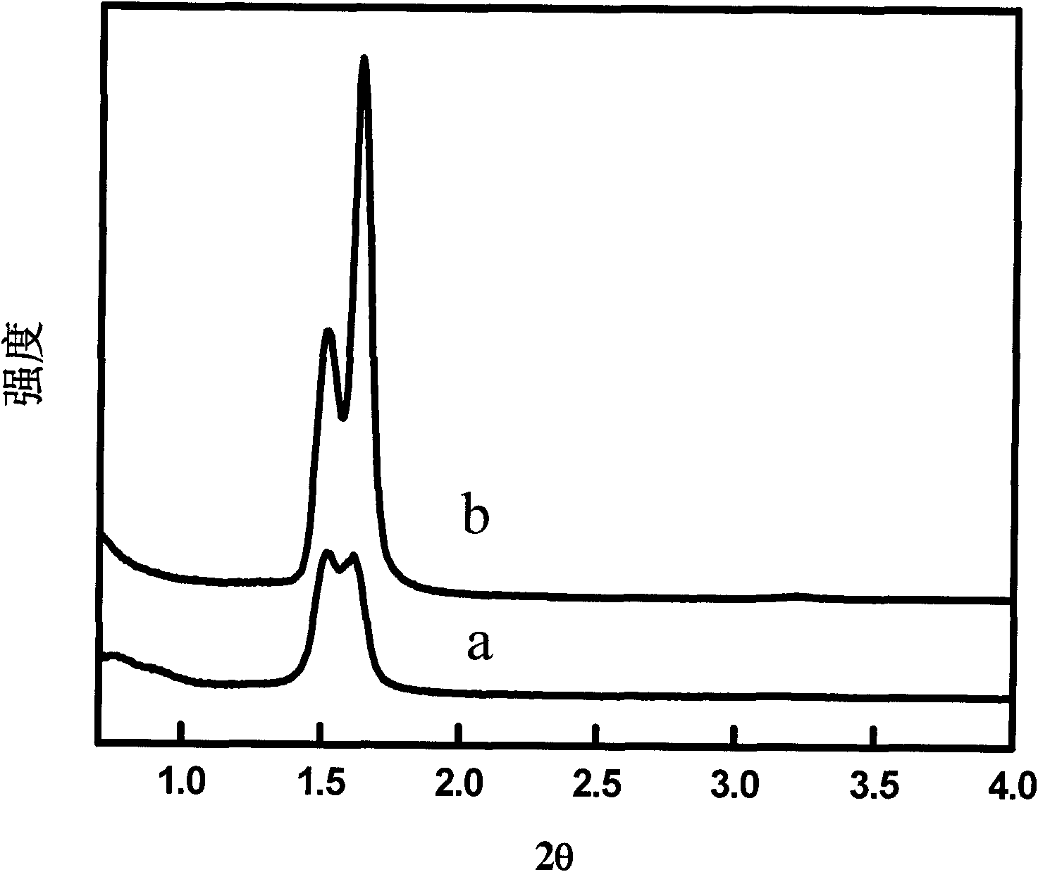
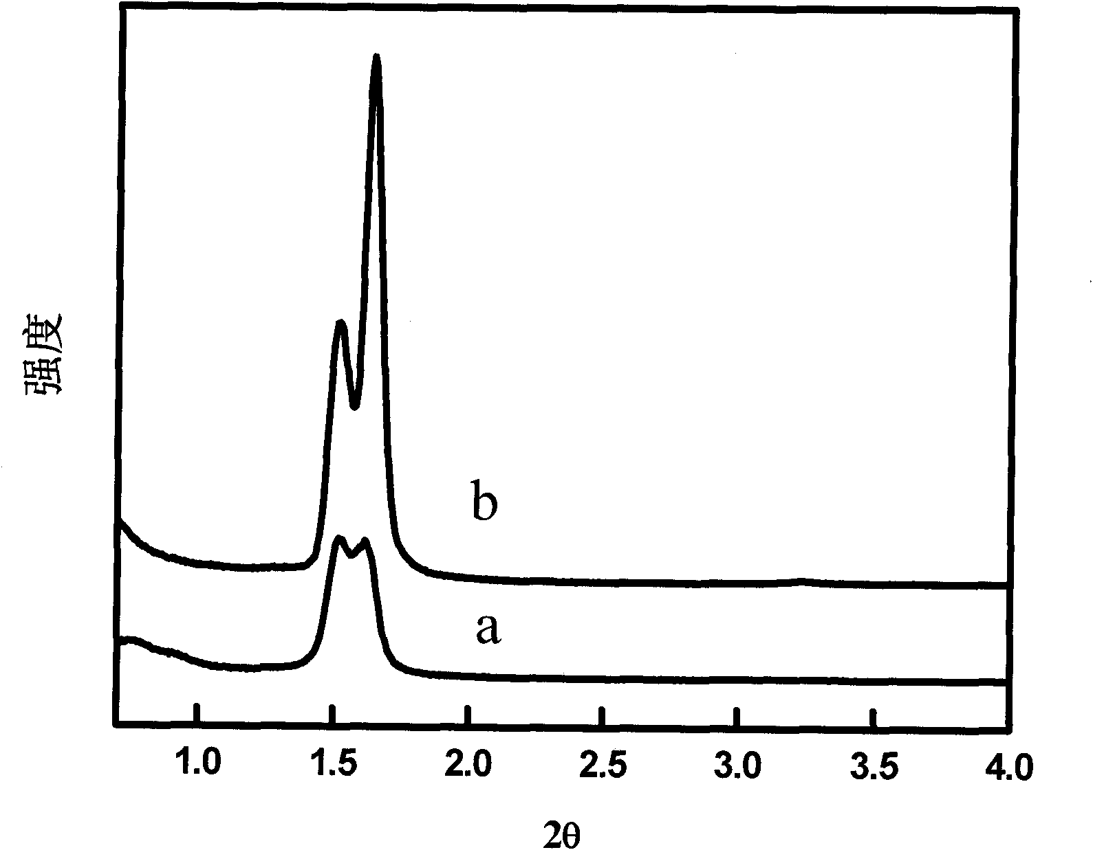
[0023] 1. Add CH 3 Si(OEt) 3 and (EtO) 3 Si-CH 2 -CH 2 -Si(OEt) 3 Mix and stir until well blended, P 123 , the mixture of hydrochloric acid, ethanol and water was stirred evenly, then added to the mixture of the precursor, and stirred in a water bath at 60° C. for 2 hours. The molar ratio of the above components in sample I is: CH 3 Si(OEt):(EtO) 3 Si-CH 2 -CH 2 -Si(OEt) 3 :P 123 :HCl:H 2 O:EtOH=0.25:0.375:1.23×10 -2 : 1.80×10 -2 :20:13.9. The molar ratio of the above components in sample II is: CH 3 Si(OEt):(EtO) 3 Si-CH 2 -CH 2 -Si(OEt) 3 :P123:HCl:H 2 O:EtOH=0.25:0.375:1.23×10 -2 : 1.80×10 -2 :20:14.37.

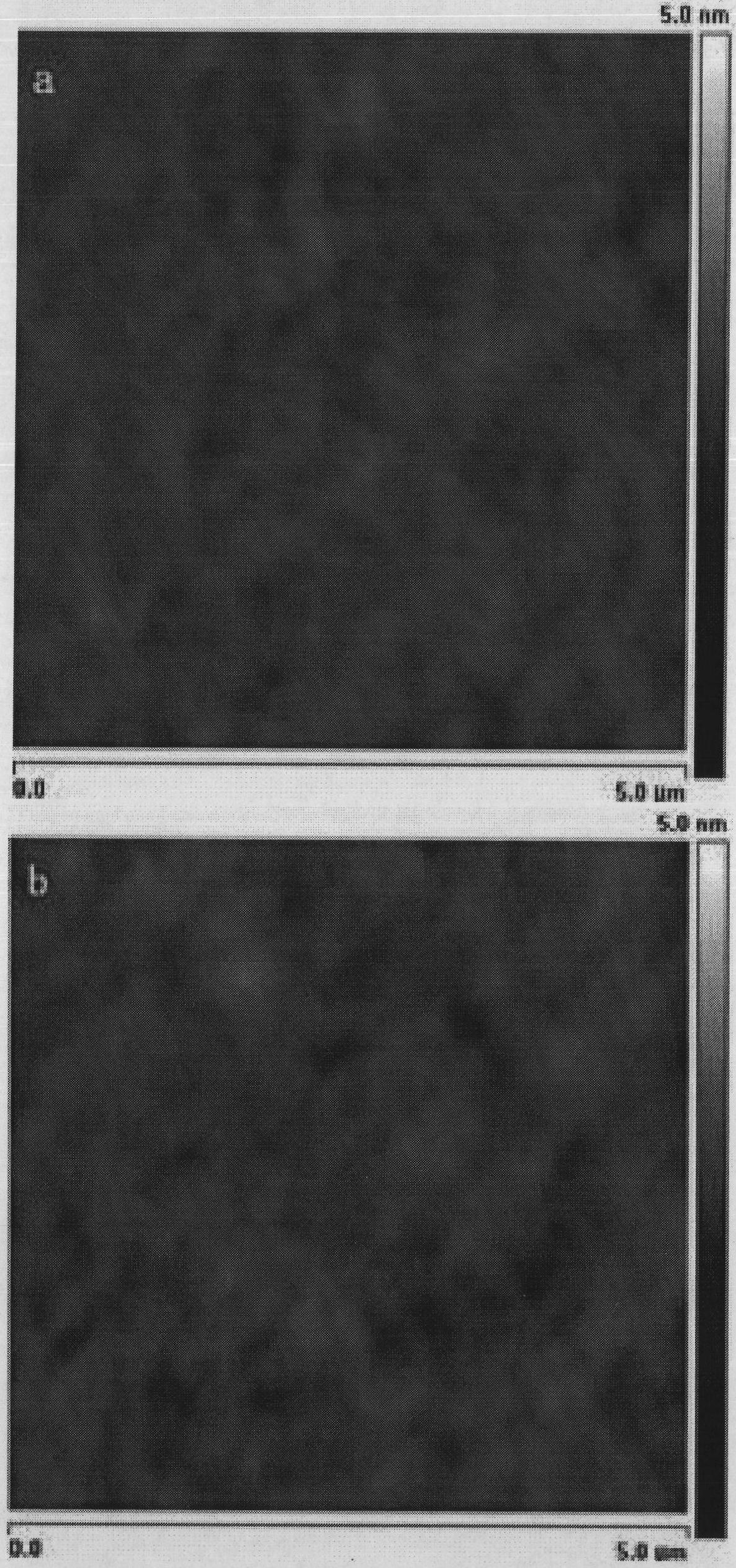
[0024] 2. Spin-coat the above-mentioned film-forming solution on a clean silicon wafer as a substrate at 25°C to form a film. The spin-coating step is as follows: first, spin at 800 rpm for 10 seconds, and then accelerate to 2000 rpm for 20 seconds. Let stand for 30-60 minutes before use.

[0025] 3. Place the above-mentioned films I and II in an ...


PUM

PropertyMeasurementUnit
thermal stabilityaaaaaaaaaa
current densityaaaaaaaaaa
diameteraaaaaaaaaa

Abstract

The invention belongs to the technical field of integrated circuit manufacture, in particular to a porous ultra-low dielectric constant material film and a preparation method thereof. The preparation procedures of the invention are as follows: using the sol-gel process, taking organo-siloxane as a precursor, and preparing the porous ultra-low dielectric constant material by controlling the ratio of the precursor to a pore forming agent, a catalyst and a solvent, the solution concentration, and the synthesis, post-treatment and annealing temperatures and the like. The process has simple procedures, and the prepared film has ordered nano-pores, even surface, low roughness and good thermal stability, the dielectric constant is 1.9-2.0, and the leakage current density is from10-8 to10-9A / cm<2>order of magnitude at 1MV / cm.

Description

technical field [0001] The invention relates to the technical field of integrated circuit manufacturing, in particular to an ultra-low dielectric constant porous material film and a preparation method thereof. Background technique [0002] With the development of integrated circuit technology, chips with high speed, high device density, low power consumption and low cost have increasingly become the main products of VLSI manufacturing. At this time, the density of wires in the chip continues to increase, the width and spacing of wires continue to decrease, and the parasitic effects generated by the resistance (R) and capacitance (C) in the interconnect become more and more obvious. Replace traditional SiO with low dielectric constant film 2 (k ~ 4.0) can not only reduce RC delay, but also reduce power consumption and signal crosstalk. At present, there are two main ways to reduce the k value of materials: one is to reduce the density of materials, and the other is to reduc...

Claims


Application Information

Patent Timeline
Patent Type & Authority Applications(China)
IPC IPC(8): H01L23/532H01L21/768
Inventor 付爽丁士进张卫
Owner FUDAN UNIV
Why Eureka
Try Eureka