Metal nano particle composite material and preparation method thereof
A technology of metal nanoparticles and composite materials, applied in the field of metal nanoparticle composite materials and their preparation, to achieve the effect of controllable physical properties and simple preparation methods
- Summary
- Abstract
- Description
- Claims
- Application Information
AI Technical Summary
Problems solved by technology
Method used
Image
Examples
preparation example Construction
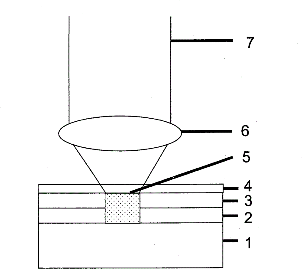
[0024] The preparation method of the metal nanoparticle composite material, the method comprises the following steps:
[0025] ① depositing the metal layer 2, the phase change material layer 3 and the protective layer 4 sequentially on the substrate 1 to form a multi-layer structure film;
[0026] ②Using laser pulses to irradiate the multilayer structure film to form a composite material 5 in which metal nanoparticles are dispersed in the phase change material.
[0027] The preparation method of composite material 5 uses magnetron sputtering equipment, and the degree of vacuum is 1.0×10 -4 Under the condition of Pa, the metal layer 2 , the phase change material layer 3 and the protection layer 4 are sequentially sputtered on the substrate 1 . Then, the nanosecond (picosecond or femtosecond) pulsed laser 7 is used to act on the multilayer film structure through the objective lens 6 with a numerical aperture of 0.9, and the metal nanoparticle composite material 5 is formed in t...
Embodiment 1
[0030] refer to figure 1 , figure 1 Schematic diagram of the preparation method of the metal nanoparticle film of the present invention. The multilayer film structure is sputtering a metal layer 2 and a phase change material layer 3 on a substrate 1 in sequence. The basic process is roughly:
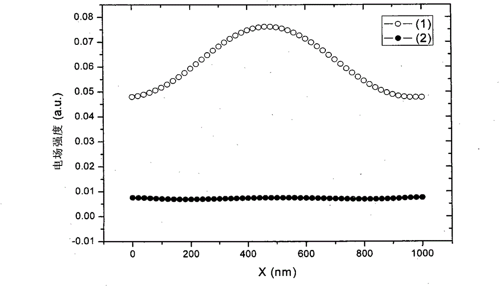
[0031] Using magnetron sputtering equipment, the vacuum degree is 1.0×10 -4 Under the condition of Pa, on the clean glass substrate 1, Ag metal layer (film thickness 40nm), Ge 2 Sb 2 Te 5 A phase change material layer (thickness: 40nm) forms a multilayer film structure. Then, a nanosecond pulsed laser 7 with a wavelength of 488nm, a pulse width of 200ns, and a power of 12mW is used to act on the multilayer film structure through an objective lens 6 with a numerical aperture of 0.9, and a metal nanoparticle composite material 5 is formed in the focused laser action area. . The near-field light distribution characteristics (numerical simulation) of the plane wave laser with a wavel...
Embodiment 3
[0033] The basic process is roughly:
[0034] The multi-layer film structure is sputtering a metal layer 2 , a phase change material layer 3 and a protective layer 4 on a substrate 1 in sequence.
[0035] Using magnetron sputtering equipment, the vacuum degree is 1.0×10 -4 Under the condition of Pa, on the clean glass substrate 1, Ag metal layer 2 (thickness 60nm), Ge 2 Sb 2 Te 5The phase change material layer 3 (film thickness 40nm) and the SiN protective layer 4 (10nm) form a multi-layer film structure. Then, a nanosecond pulsed laser 7 with a wavelength of 488nm, a pulse width of 200ns, and a power of 12mW is used to act on the multilayer film structure through an objective lens 6 with a numerical aperture of 0.9, and a metal nanoparticle composite material 5 is formed in the focused laser action area. .
[0036] The specific preparation process parameters of other embodiments are shown in Table 1 below, and I will not repeat the description.
[0037] Table 1
[0038...
PUM
| Property | Measurement | Unit |
|---|---|---|
| thickness | aaaaa | aaaaa |
| thickness | aaaaa | aaaaa |
| thickness | aaaaa | aaaaa |
Abstract
Description
Claims
Application Information

