Manufacturing method of film material for solar cells

A technology of solar cells and thin film materials, applied in the direction of final product manufacturing, sustainable manufacturing/processing, circuits, etc., can solve the problems of high manufacturing cost, attenuation of photoelectric conversion efficiency, and low conversion efficiency

Active Publication Date: 2010-08-11
胡倾宇
View PDF7 Cites 6 Cited by
  • Summary
  • Abstract
  • Description
  • Claims
  • Application Information

AI Technical Summary

Problems solved by technology

[0006] Amorphous silicon thin-film solar cells were successfully developed by Carlson and Wronski in the mid-1970s, and their production reached a peak in the 1980s, accounting for about 20% of the total global solar cells. However, due to the lower conversion efficiency of amorphous silicon solar cells Crystalline silicon solar cells, and amorphous silicon solar cells have the disadvantage of light-induced attenuation effect: the photoelectric conversion efficiency will decay with the

Method used


Image

  • Manufacturing method of film material for solar cells
  • Manufacturing method of film material for solar cells
  • Manufacturing method of film material for solar cells

Examples


example 1

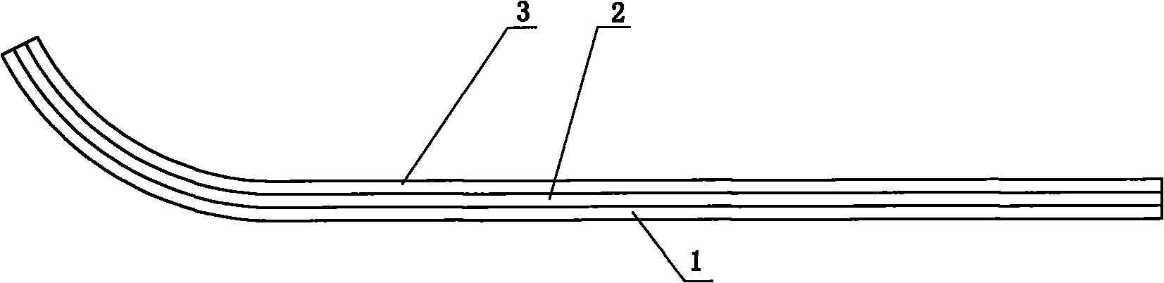
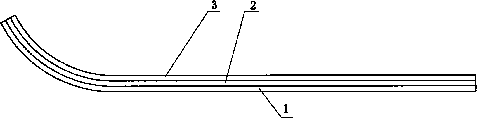
[0038] Example 1, using a 0.25 mm thick Hastelloy 276 substrate layer 1 after electrochemical polishing, using vacuum electron beam evaporation technology and inclined substrate deposition method to prepare a layer of 1 micron MgO and 1 micron yttrium oxide Y at room temperature 2 o 3 Template film layer 2, and then grow a layer of 50 nm CeO 2 , the Si semiconductor thin film layer 3 is prepared by chemical vapor deposition CVD under the condition of 600-800°C. The X-ray rocking curve FWHM used to evaluate the texture degree of the film along the plane of the film is only 7°, and the texture degree is very good.

example 2

[0039] Example 2, using the 1.00 mm thick Hastelloy 276 substrate layer 1 after electrochemical polishing, using vacuum electron beam evaporation technology and inclined substrate deposition method to prepare a layer of 1 micron MgO and 1 micron yttrium oxide Y at room temperature 2 o 3 Template film layer 2, and then grow a layer of 50 nm CeO 2 , the gallium arsenide GaAs semiconductor thin film layer 3 is prepared by chemical vapor deposition CVD under the condition of 700-900° C., and the FWHM is 9°.

example 3

[0040] Example 3, the 0.8 mm thick stainless steel sheet substrate layer 1 after mechanical polishing was polished, and a layer of 1 micron MgO and 1 micron yttrium oxide Y were prepared at room temperature using vacuum electron beam evaporation technology and inclined substrate deposition method. 2 o 3 Template film layer 2, and then grow a layer of 50 nm CeO 2 , and finally the GaAs semiconductor thin film layer 3 is epitaxially grown by pulsed laser deposition at 700-800° C. under vacuum, with a FWHM of 9°.


PUM

PropertyMeasurementUnit
Thicknessaaaaaaaaaa

Abstract

The invention relates to a manufacturing method of a film material for solar cell panels, in particular to a manufacturing method of a film material for solar cells. The film material comprises a substrate layer (1), a template film layer (2) and a semiconductor film layer (3) from bottom to top, wherein the substrate layer (1) is sheet metal, ceramic or glass in a non-crystalline or polycrystalline structure; the template film layer (2) is in a crystallographic biaxial texture structure and is prepared by an inclined substrate deposition method; and the semiconductor film layer (3) is prepared by physical vapor deposition or chemical vapor deposition, is formed by epitaxial growth of the template film layer, is in a crystallographic biaxial texture structure, and is in a photovoltaic conversion structure formed by connecting one or a plurality of P-N joints in series. In the invention, the thickness of the semiconductor layer for solar cells is only 1-10 micrometers, thereby saving 98% of silicon semiconductor materials; compared with non-crystalline solar cells, the solar conversion efficiency can be improved by 12%; the invention has the advantages of simple equipment, high efficiency and low cost; and the template film layer (2) has a certain roughness, sunlight can be fully absorbed, and the absorption efficiency and the conversion efficiency of the solar cells can be improved.

Description

(1) Technical field [0001] The invention relates to a manufacturing method of a solar battery panel, in particular to a manufacturing method of a thin film material used in a solar battery panel. (2) Background technology [0002] Traditional fuel energy is decreasing day by day, and the damage to the environment is becoming more and more prominent. At the same time, there are still 2 billion people in the world who do not have normal energy supply. Therefore, the whole world has turned its attention to renewable energy, hoping that renewable energy can change the energy structure of mankind and maintain the long-term sustainable development of human society. Among them, solar energy has become the focus of people's attention due to its unique advantages. Solar radiation is essentially the source of most energy sources on the earth. It is an inexhaustible, non-polluting, cheap energy source that humans can use freely. The energy of solar energy reaching the ground every se...

Claims


Application Information

Patent Timeline
IPC IPC(8): H01L31/18
CPCY02P70/50
Inventor 胡倾宇
Owner 胡倾宇
Why Eureka
Try Eureka