Capacitor composed by utilizing semiconductor PN junction capacitance and manufacturing method thereof

A fabrication method and semiconductor technology are applied in the field of capacitors to achieve the effects of simple structure, small parasitic parameters and high capacitance density

Active Publication Date: 2010-08-25
NAT CENT FOR ADVANCED PACKAGING
View PDF0 Cites 9 Cited by
  • Summary
  • Abstract
  • Description
  • Claims
  • Application Information

AI Technical Summary

Problems solved by technology

[0007] The capacitance formed by the large-area PN junction is directly made into a decoupling capacitor in an independent form, and it has not been reported in an electronic package or system for intermediate frequency decoupling in a surface-mounted manner.

Method used


Image

  • Capacitor composed by utilizing semiconductor PN junction capacitance and manufacturing method thereof
  • Capacitor composed by utilizing semiconductor PN junction capacitance and manufacturing method thereof
  • Capacitor composed by utilizing semiconductor PN junction capacitance and manufacturing method thereof

Examples


Embodiment Construction

[0068] In order to make the object, technical solution and advantages of the present invention clearer, the present invention will be described in further detail below in conjunction with specific embodiments and with reference to the accompanying drawings.

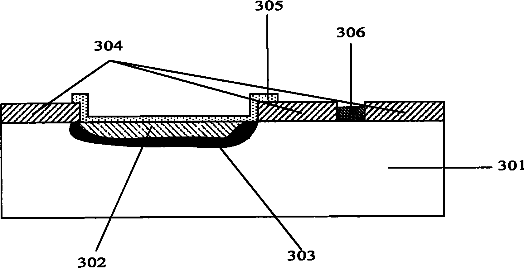
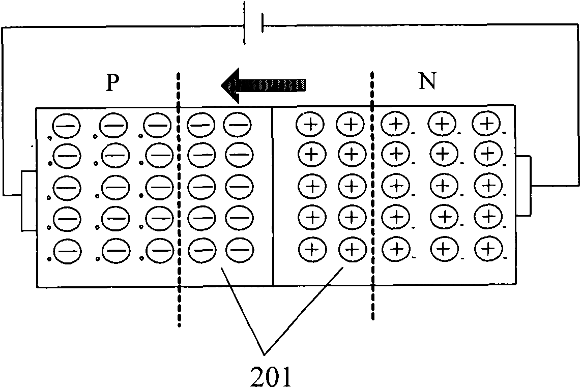
[0069] The invention uses semiconductor PN junction capacitance to replace traditional MIM "sandwich" structure capacitance, utilizes its characteristics of good high-frequency characteristics and small reverse leakage current, and is applied to decoupling circuits. The PN junction capacitance of a semiconductor includes two parts, the barrier capacitance and the diffusion capacitance. The barrier capacitance is due to the change of the applied voltage on the PN junction, which causes the "storage" and "extraction" of electrons and holes in the barrier region. , resulting in the amount of space charge in the barrier region changing with the applied voltage, which is equivalent to the charging and discharging effect of a ca...


PUM


Abstract

The invention discloses a capacitor composed by utilizing a semiconductor PN junction capacitance and a manufacturing method thereof. The capacitor utilizes a semiconductor as a base material, and the capacitance of the capacitor is the semiconductor PN junction capacitance. The capacitor comprises a PN junction, a metal film layer, an electrode bump and an extraction electrode, wherein the PN junction is formed in a specific area by utilizing a diffusion method or an ion implantation method on a high-doping and low-resistance P type or N type semiconductor base material; the metal film layer is manufactured by utilizing a thermal evaporation method, an electron beam evaporation method or a sputtering method on the N type area or the P type area of the semiconductor forming the PN junction; the electrode bump is manufactured by an electroplating method or a screen printing method on the metal film; and the extraction electrode can be arranged on both faces of the semiconductor base material or only on a corrosion area face. The capacitor manufactured by the method of the invention has the characteristics of simple structure, large capacitance density, small parasitic parameters and simple manufacturing technical process, and also has protection function on static electricity and surging, thus being capable of being widely applied to electronic systems with high frequency, high speed and high power.

Description

technical field [0001] The invention relates to the technical field of microelectronic devices, in particular to a capacitor composed of semiconductor PN junction capacitance mainly used in occasions such as intermediate frequency (200MHz-2.5GHz) decoupling and a manufacturing method thereof. Background technique [0002] Decoupling capacitors are widely used in various electronic systems. They are generally connected between the power supply and the ground in the power supply network in the electronic system. Using the principle that the higher the capacitance frequency, the smaller the impedance, the high-frequency noise in the power supply network Reduced, thereby suppressing the noise in the power network. [0003] In practical applications, due to the inherent parasitic inductance and resistance of capacitors, it is impossible for any kind of capacitor to achieve full-band decoupling from low frequency to high frequency. Generally speaking, the larger the capacitance o...

Claims


Application Information

Patent Timeline
Patent Type & Authority Applications(China)
IPC IPC(8): H01L29/92H01L21/329
Inventor 万里兮吕垚李宝霞
Owner NAT CENT FOR ADVANCED PACKAGING
Why Eureka
Try Eureka