
Composite plane terminal passivating method for controllable silicon device

A composite planar and silicon device technology, applied in semiconductor/solid-state device manufacturing, electrical components, circuits, etc., can solve the problem that the gate trigger current is difficult to guarantee the off-state repetitive peak voltage, the mesa process terminal passivation process is cumbersome, and the mesa process Problems such as poor parameter consistency, to achieve the effect of shortening the production cycle, small proportion, and shortening the production process

Active Publication Date: 2012-01-04
江苏新顺微电子股份有限公司
View PDF0 Cites 0 Cited by
  • Summary
  • Abstract
  • Description
  • Claims
  • Application Information

AI Technical Summary

Problems solved by technology

[0010] 1. The terminal passivation process of the countertop process is cumbersome
[0011] Although the countertop technology is relatively mature, the process is very complicated and requires groove photolithography, glass electrophoresis, glass sintering, glass protection, and glass reverse etching
[0012] 2. High fragmentation rate of countertop technology: 10%-20%
[0014] 3. The consistency of the process parameters of the table is poor, and the gate trigger current (I GT ), off-state repetitive peak voltage (V DRM ) is difficult to guarantee
[0015] The mesa process relies on glass passivation to ensure the breakover voltage, and glass is easily corroded. Once there is a problem with the protective layer, the chip is easily scrapped
[0016] 4. The structure design of the mesa terminal accounts for a large proportion of the chip area
[0017] In summary, the disadvantages of the mesa passivation process are that the processing process is complex, parameter control is difficult, the chip is fragile after the silicon etching groove is filled with glass, and the mesa terminal structure occupies a much larger proportion of the chip area than the planar process.

Method used


Image

  • Composite plane terminal passivating method for controllable silicon device
  • Composite plane terminal passivating method for controllable silicon device
  • Composite plane terminal passivating method for controllable silicon device

Examples


Embodiment Construction

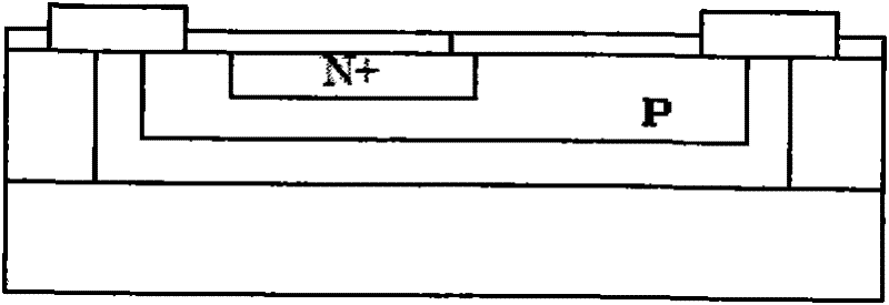
[0047] The planar terminal passivation method of the thyristor device involved in the present invention is to use a composite film generated by chemical vapor deposition as the terminal passivation structure of the thyristor device, and the method includes the following process:

[0048] Step 1, at a certain temperature (1150~1250 ℃), time (the specific time is determined by I GT set) and atmosphere (N 2 : 10L / min, O 2 : 1L / min), the phosphorus atoms are pushed into the silicon chip to a certain depth to form the cathode area, and the oxidation diffusion of the cathode area of ​​the chip is completed, such as Figure 6 shown.

[0049] Step 2. The silicon wafer that has been oxidized and diffused in the cathode area of ​​the chip is completely peeled off by using a silicon dioxide etching solution to form a silicon substrate layer of the chip, such as Figure 7 shown.

[0050] Step 3, adopt the method of chemical vapor deposition (600-700 ℃, 20-60pa lower N 2 O and SiH 4 ...


PUM


Abstract

The invention relates to a composite plane terminal passivating method for a controllable silicon device. The method comprises the following processes: 1, pushing phosphorus atoms into a silicon chip in a certain depth under certain temperature, time and atmosphere to form a gate region so as to finish oxidation and diffusion of a cathode region of the chip; 2, fully peeling an oxidation layer onthe surface of the silicon chip to form a chip silicon substrate layer; 3, depositing a passivation layer on the surface of the chip silicon substrate layer formed in the step 2; 4, depositing a first protective layer, a second protective layer and a third protective layer on the surface of the passivation layer formed in the step 3 in turn to form a passivating film protective PN junction terminal; and 5, annealing the passivating film protective PN junction terminal formed in the step 4 for certain time, and engraving a cathode and gate pole lead hole window at the passivating film protective PN junction terminal through photo-etching so as to finish passivation of the controllable silicon plane terminal. The method can improve the parameter stability and controllability of a controllable silicon product, reduce the area of the chip, shorten the production flow, reduce the fragment rate and reduce the production cost.

Description

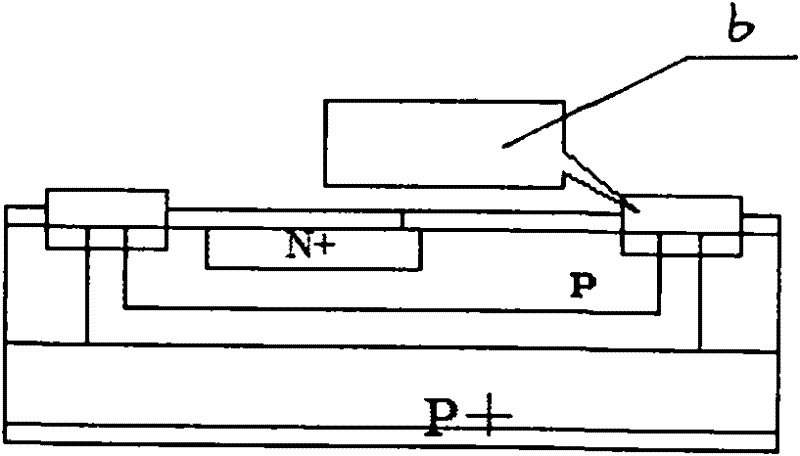
(1) Technical field [0001] The invention relates to a plane processing method of a thyristor device. It belongs to the technical field of discrete device processing technology. (2) Background technology [0002] In recent years, the demand for consumable products of thyristor devices has increased greatly, and their types have also increased accordingly, and product competition has become increasingly fierce. How to improve parameter consistency, reduce fragmentation rate, and reduce production cost under the condition of ensuring reliability has become the goal pursued by chip manufacturers. [0003] Before the present invention was made, shallow mesa technology was widely used in the production field of thyristor devices. Its processing technology is as follows: [0004] Step 1. Under a certain temperature, time and atmosphere, push phosphorus atoms to a certain depth on the surface of the silicon wafer to form a gate area, such as figure 1 shown. [0005] Step 2, car...

Claims


Application Information

Patent Timeline
Patent Type & Authority Patents(China)
IPC IPC(8): H01L21/332
Inventor 王新潮冯东明高善明李建立
Owner 江苏新顺微电子股份有限公司
Learn More