Laser light source device of high-power semiconductor

A laser light source, semiconductor technology, applied in semiconductor laser devices, laser devices, devices for controlling laser output parameters, etc., can solve the problems of short life, large volume, low energy efficiency, etc. quality effect

Inactive Publication Date: 2010-10-06
长春德信光电技术有限公司
View PDF4 Cites 16 Cited by
  • Summary
  • Abstract
  • Description
  • Claims
  • Application Information

AI Technical Summary

Problems solved by technology

[0009] The problem to be solved by the present invention is to overcome the CO 2 The base frequency 1064nm Nd:YAG lasers pumped by lasers, lamp pumps and semiconductor lasers have the disadva

Method used


Image

  • Laser light source device of high-power semiconductor
  • Laser light source device of high-power semiconductor
  • Laser light source device of high-power semiconductor

Examples


Embodiment 1

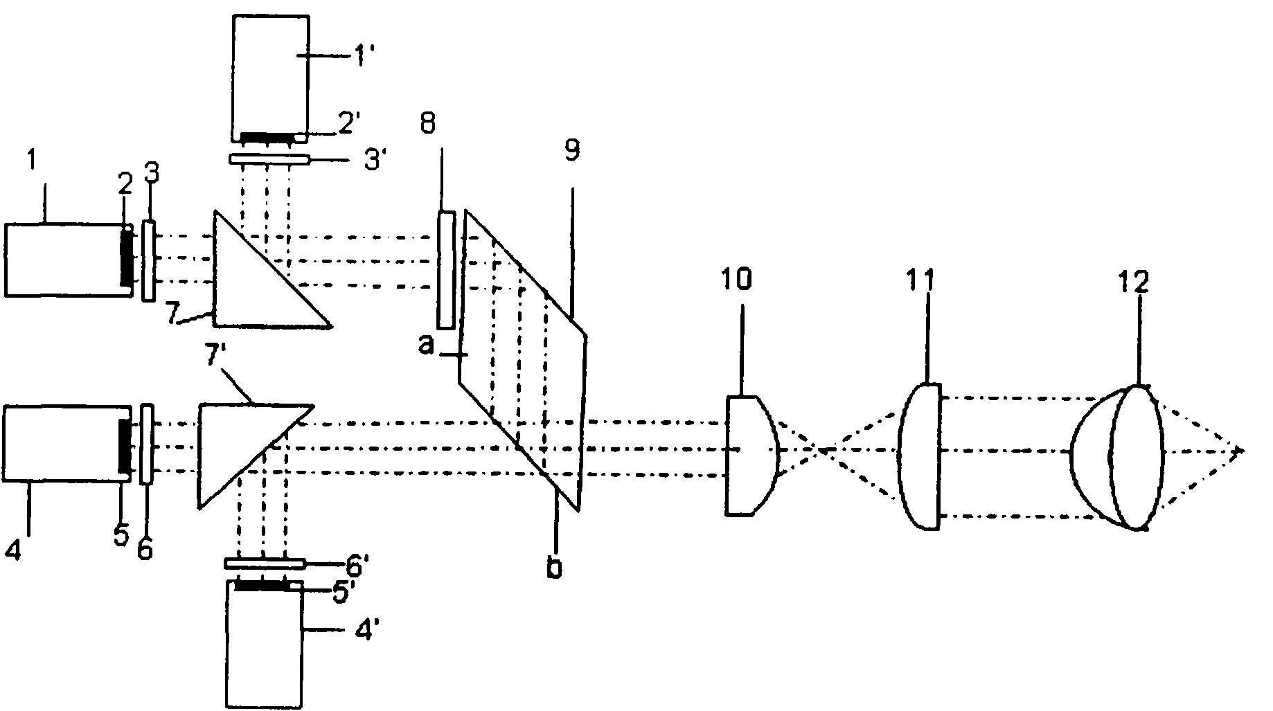
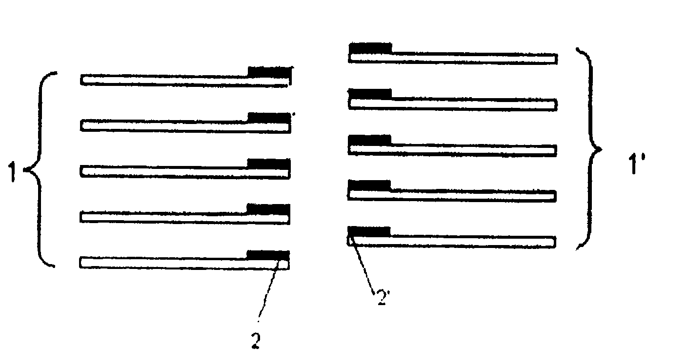
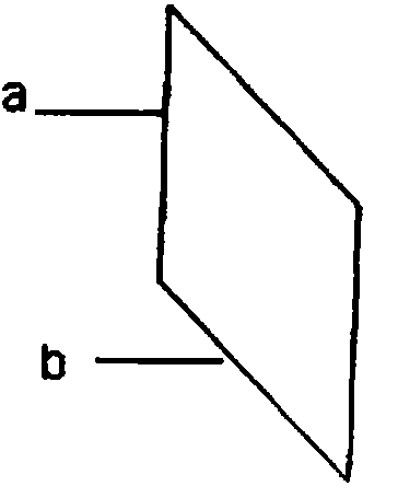
[0037] like figure 1Shown, the high-power semiconductor laser light source device that the present invention provides is by first semiconductor laser stack 1, the second semiconductor laser stack 1 ', the 3rd semiconductor laser stack 4, the 4th semiconductor laser stack 4 '; Fast axis collimating lens 2, second fast axis collimating lens 2', third fast axis collimating lens 5, fourth fast axis collimating lens 5'; first slow axis collimating lens 3, second slow axis collimating lens Straight lens 3', the third slow axis collimating lens 6, the fourth slow axis collimating lens 6'; the first isosceles right triangle reflective prism 7, the second isosceles right triangle reflective prism 7'; half wave plate 8; A rhombic polarizing coupling prism 9; a beam expander system composed of a first cylindrical lens 10 and a second cylindrical lens 11 and a focusing system 12 composed of a doublet lens;

[0038] The first fast-axis collimating lens 2, the second fast-axis collimating ...


PUM


Abstract

The invention relates to a laser light source device of a high-power semiconductor. A laser light source with high power, high light beam quality and small divergence angle is obtained by adopting a plurality of hectowatt-level laser stack array module through a beam binding technology and a beam expanding focusing technology. The laser light source device has light weight, small volume, high electro-optic conversion efficiency and long service life, overcomes the disadvantages of big volume, low energy efficiency, short service life and the like of chemical lasers, CO2 lasers and the fundamental frequency 1064nm Nd:YAG lasers of lamp pumps and semiconductor laser pumping and the like, realizes the high-power, high-brightness and high-quality direct input of the hectowatt-level lasers and can be directly applied to the field of laser processing. Under the condition of the same output power, the volume of a semiconductor laser is 1/3-1/10 the volume of other lasers, the operating cost thereof is 1/4-1/20 the costs of other lasers, and the service life thereof is 5-10 times the service lives of other lasers and can reach more than 10000 hours.

Description

technical field [0001] The invention relates to a high-power semiconductor laser light source device whose output power can be as high as several thousand watts. Background technique [0002] Because high-power semiconductor lasers have the advantages of small size, light weight, high efficiency, and long life, they have been widely used in laser processing (drilling, cutting, welding, surface processing, material modification, etc.), laser medical treatment (diagnosis, treatment, Surgery, cosmetology, etc.), laser display and scientific research, etc., have become comprehensive high-tech in the new century with rapid development, many achievements, wide penetration of disciplines, and wide application range. [0003] At present, CO is mostly used in laser processing 2 Lasers, lamp-pumped and semiconductor laser-pumped fundamental frequency 1064nm Nd:YAG lasers. [0004] CO 2 Lasers, by converting the thermal energy of combustion gases into laser energy, achieve megawatt-...

Claims


Application Information

Patent Timeline
IPC IPC(8): H01S5/40H01S5/06
Inventor 顾媛媛王峙皓甘露
Owner 长春德信光电技术有限公司
Why Eureka
Try Eureka