Lithium ion secondary battery cathode, preparation method thereof and lithium ion secondary battery
A secondary battery and lithium ion technology, which is applied in secondary batteries, electrode manufacturing, battery electrodes, etc., can solve the problems of poor battery cycle performance, improve battery cycle performance, solve the problem of poor battery cycle performance and increase battery capacity Effect
- Summary
- Abstract
- Description
- Claims
- Application Information
AI Technical Summary
Problems solved by technology
Method used
Image
Examples
preparation example Construction
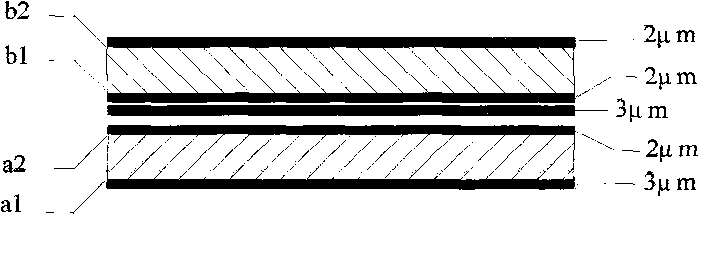
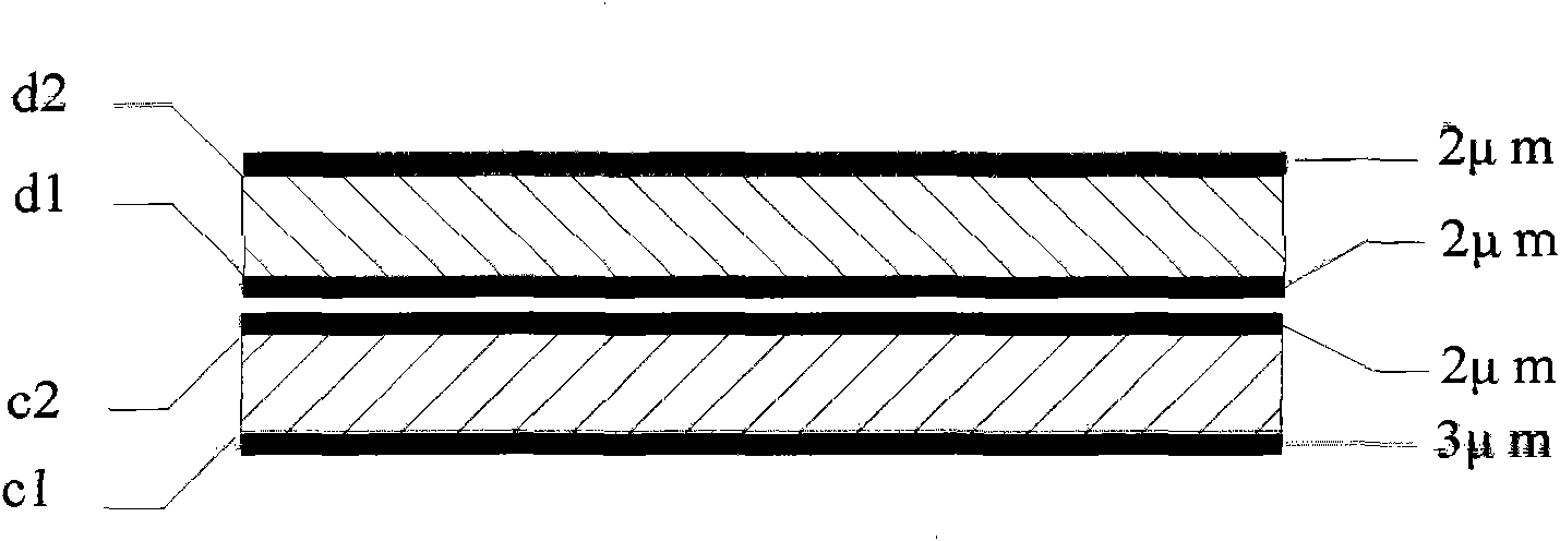
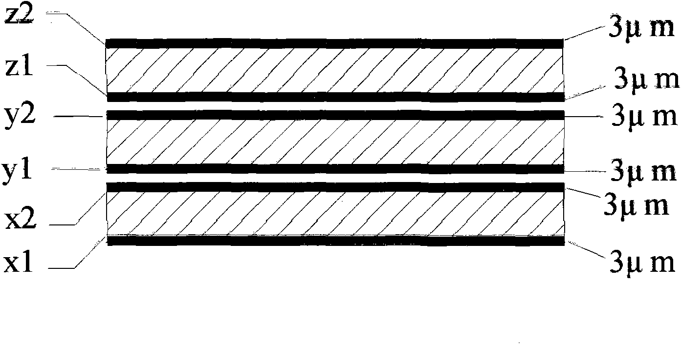
[0025] The method for preparing the through hole on the silicon film is not particularly limited, and one of the following two methods can be selected. Method 1: First use physical vapor deposition, such as electron beam evaporation, RF sputtering, etc., to deposit powdered silicon on the surface of the negative electrode collector to form a layer of silicon film. A multi-layer silicon film is formed on the surface. Then, the anode current collector with the silicon thin film deposited on the surface is punched with a punching device, so that both the silicon thin film and the anode current collector have through holes. The specific embodiment of the present invention uses a laser drilling device to drill holes. If the laser drilling is performed in air, the silicon near the through hole on the silicon film will be partially oxidized. The inventors have found that when the average pore diameter and the average pore density of the through holes according to the specific embodi...
Embodiment 1
[0037] 1. Preparation of negative electrode
[0038] 1.1 Deposition of amorphous silicon thin film:
[0039] Three copper foils of the same specification were selected as negative electrode collectors. The length and width of the copper foil are 480mm and 44mm respectively, and the thickness is 15μm. The roughness of both sides of the copper foil is R Z = 2.5 μm. Using electron beam evaporation method (EB-PVD vacuum evaporation apparatus), use silicon powder (amorphous) with a purity of 99.99% as raw material to evaporate a layer of silicon film with a thickness of 6 μm on both surfaces of each copper foil . The obtained silicon thin film is an amorphous silicon thin film. The working voltage of EB-PVD is 7000V, the working current is 120mA, and the working pressure of the vacuum chamber is 0.05 millitorr.
[0040] 1.2 Amorphous silicon thin film drilling:
[0041] Stack the 3 copper foils with amorphous silicon films deposited on both surfaces obtained in step 1.1, and ...
Embodiment 2
[0057] According to the method of Example 1, the difference is: the negative electrode current collector is a beryllium bronze alloy copper foil with a thickness of 18 μm, the number is 2, and the roughness of both sides is equal, both of which are R Z = 3.5 μm; during electron beam evaporation, the vacuum degree is 0.08 millitorr; the thickness of each layer of amorphous silicon film deposited on the surface of the negative electrode current collector is 5 μm; the average pore diameter of the through holes on the silicon film is 0.2 mm, and the average hole density is 5 piece / mm 2 . The resulting negative electrode structure was figure 2 Similar, except that the thickness of each layer of amorphous silicon film deposited on the surface of the negative electrode current collector is the same, and both are 5 μm.
[0058] The theoretical discharge capacity of the battery negative electrode material is 950mAh / g, the actual discharge capacity of the battery negative electrode m...
PUM
| Property | Measurement | Unit |
|---|---|---|
| Thickness | aaaaa | aaaaa |
| Average pore size | aaaaa | aaaaa |
| Surface roughness | aaaaa | aaaaa |
Abstract
Description
Claims
Application Information


