Crystallization of amorphous silicon film as well as manufacture method and device of poly-silicon film

An amorphous silicon thin film and crystallization technology, applied in semiconductor/solid-state device manufacturing, electrical components, circuits, etc., can solve the problems of complex laser crystallization process, difficult maintenance, affecting TFT uniformity, etc., to improve electron mobility , Save the cost of use, eliminate the effect of lattice defects

Inactive Publication Date: 2013-04-17
SHENZHEN DANBANG INVESTMENT GROUP
View PDF4 Cites 2 Cited by
  • Summary
  • Abstract
  • Description
  • Claims
  • Application Information

AI Technical Summary

Problems solved by technology

[0007] In the process of crystallizing amorphous silicon thin film into polycrystalline silicon thin film, many variables have a direct impact on the grain size and distribution after crystallization, such as the film quality of amorphous silicon thin film, the size of laser energy density, laser The uniformity of energy distribution in space, the degree of overlap of laser pulses, the temperature of the substrate during laser annealing, and the surrounding atmosphere, etc., when the control of the process is not ideal, many small channels will be generated in the active channel area after crystallization. The polysilicon thin film grains, and then derive a large number of grain boundaries, and then affect the uniformity of TFT, so the laser crystallization process is complicated
[0008] In addition, excimer laser crystallization has several serious disadvantages
For example, the radiation heat of the laser beam itself in the laser system, the extremely limited processing range of the laser process, and the crystallization equipment using the excimer laser are complex and costly, and the life of the excimer laser is short and difficult to maintain and many more

Method used


Image

  • Crystallization of amorphous silicon film as well as manufacture method and device of poly-silicon film
  • Crystallization of amorphous silicon film as well as manufacture method and device of poly-silicon film
  • Crystallization of amorphous silicon film as well as manufacture method and device of poly-silicon film

Examples


Embodiment 1

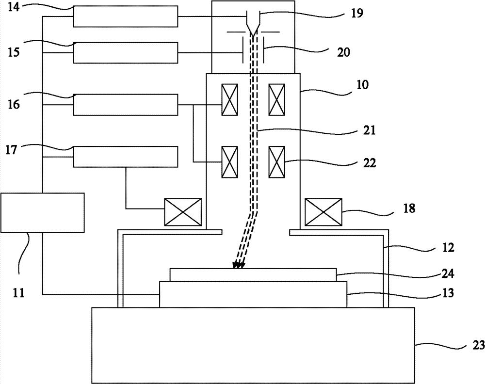
[0040] In this example, the electron beam crystallization device is as image 3 As shown, it mainly includes: an electron optical system 10, a computer control system 11, a vacuum workpiece chamber 12 and a workpiece console 13 placed in the workpiece chamber, and the vacuum workpiece chamber is placed on a shockproof table 23. The electron optical system is placed above the workpiece chamber and works in electron beam scanning mode. Computer control system 11 controls high-voltage power supply 14 , grid power supply 15 , electron lens power supply 16 , deflection coil control 17 and workpiece console 13 .

[0041] Among them, the electron optical system is composed of a cathode 19, a grid 20, an electron lens 22, and a deflection coil 18. The cathode emits an electron beam 21, the grid controls the on-off of the electron beam, the electron lens realizes the focusing of the electron beam, and the deflection coil is fixed on the workpiece. The outer or inner walls of the chamb...

Embodiment 2

[0048] In this example, the electron beam crystallization device is as Figure 4 As shown, it mainly includes: an electron optical system 31, a computer control system 40, a vacuum workpiece chamber 29 and a workpiece console 26 placed in the workpiece chamber, and the vacuum workpiece chamber is placed on the anti-vibration table 25. The electron optical system is placed above the vacuum workpiece chamber and works in electron beam scanning mode. The computer control system controls the high-voltage power supply 36, the grid power supply 37, the electron lens power supply 38, the deflection coil control 39 and the workpiece console.

[0049] Among them, the electron optical system is composed of a cathode 35, a grid 34, an electron lens 33, and a deflection coil 30. The cathode emits an electron beam 32, the grid controls the on-off of the electron beam, the electron lens realizes the focusing of the electron beam, and the deflection coil is fixed on the workpiece. The outer...

Embodiment 3

[0058] In this example, the electron beam crystallization device is as Figure 5 As shown, it mainly includes: an electron optical system 47, a computer control system 56, a workpiece chamber 44 and a workpiece console 42 placed in the workpiece chamber. The electron optical system is placed above the workpiece chamber and is vacuum-sealed with the workpiece chamber. The electron optical system works in electron beam scanning mode. The computer control system controls the high voltage power supply 52 , the grid power supply 53 , the electron lens power supply 54 , the deflection coil control 55 and the workpiece console 42 .

[0059] Among them, the electron optical system is composed of a cathode 51, a grid 50, an electron lens 49, and a deflection coil 45. The cathode emits an electron beam 48, the grid controls the on-off of the electron beam, the electron lens realizes the focusing of the electron beam, and the deflection coil is fixed on the workpiece. The outer or inner...


PUM


Abstract

The invention relates to the crystallization of amorphous silicon films as well as manufacture method and device of poly-silicon films. In the method, electron beams of high energy density are used to act on amorphous silicon films to control the electron beams to accelerate anode voltage and beam flow so that amorphous silicon melt layers and glass base plates keep in extremely high temperature gradient. After the electron beams are stopped, the amorphous silicon melt layers are gradually cooled and crystallized. The device mainly comprises an electron-optical system, a computer control system, a workpiece chamber and a workpiece control table placed in the workpice chamber. A cathode is placed in a negative high voltage end, amorphous silicon is grounded, the electron beams scan line byline, the repetition rate on scanning the last line and the next line by the electron beams can reach above 99%, the electron beams are cut off after one round is scanned, the workpiece control tableis moved for the next round of scanning, and the process is thus repeated. The workpiece chamber can be a vacuum chamber or is in an atmosphere condition or a certain atmosphere. If in the atmosphereor inert gas environment, an electron beam leading window is arranged between the workpiece chamber and the electron-optical system.

Description

technical field [0001] The invention relates to a method and device for crystallizing an amorphous silicon film, and a method and device for manufacturing a polysilicon film using the method and device. Background technique [0002] Organic light-emitting diodes (OLEDs) have attracted much attention in the industry due to their advantages such as self-illumination, wide viewing angle, high response speed, flexibility and high brightness. Organic light emitting diodes can be classified into active organic light emitting diodes (AMOLED) and passive organic light emitting diodes (PMOLED) according to their driving methods. AMOLED uses a thin film transistor array formed on a transparent insulating substrate to control the light-emitting state of its organic light-emitting layer. [0003] Compared with traditional amorphous silicon (α-Si) thin film transistors, low-temperature polysilicon thin film transistors (LTPS TFTs) have higher electron mobility, fast response speed, shor...

Claims


Application Information

Patent Timeline
Patent Type & Authority Patents(China)
IPC IPC(8): H01L21/263H01L21/00
Inventor 刘萍
Owner SHENZHEN DANBANG INVESTMENT GROUP
Why Eureka
Try Eureka