Gallium nitride schottky rectifier with metal substrate and production method thereof
A metal substrate, gallium nitride technology, applied in the field of gallium nitride Schottky rectifier and its preparation, can solve the problems of device temperature burnout, poor thermal conductivity, affecting device stability, etc., to solve heat dissipation problems, improve performance and The effect of reliability
- Summary
- Abstract
- Description
- Claims
- Application Information
AI Technical Summary
Problems solved by technology
Method used
Image

Examples
preparation example Construction
[0032] The preparation method of the gallium nitride schottky rectifier on the metal substrate comprises the following steps:
[0033] 1) The epitaxial layer of the GaN Schottky rectifier wafer is grown on the sapphire substrate 101. The epitaxial structure includes a buffer layer 102a, a heavily doped GaN ohmic contact layer 102b and a lightly doped GaN ohmic contact layer 102b on the substrate from bottom to top GaN voltage blocking layer 102c;
[0034] 2) Fabricate a GaN Schottky rectifier wafer with a lateral structure using a semiconductor micromachining method, including: using a mesa etching method to expose the heavily doped GaN ohmic contact layer 102b at the position where the ohmic electrode 104 is set; An ohmic electrode 104 is prepared on the gallium nitride ohmic contact layer 102b, a gallium nitride Schottky electrode 103 is prepared on the lightly doped gallium nitride voltage barrier layer 102c, and the prepared gallium nitride Schottky electrode 103 and the o...
Embodiment 1
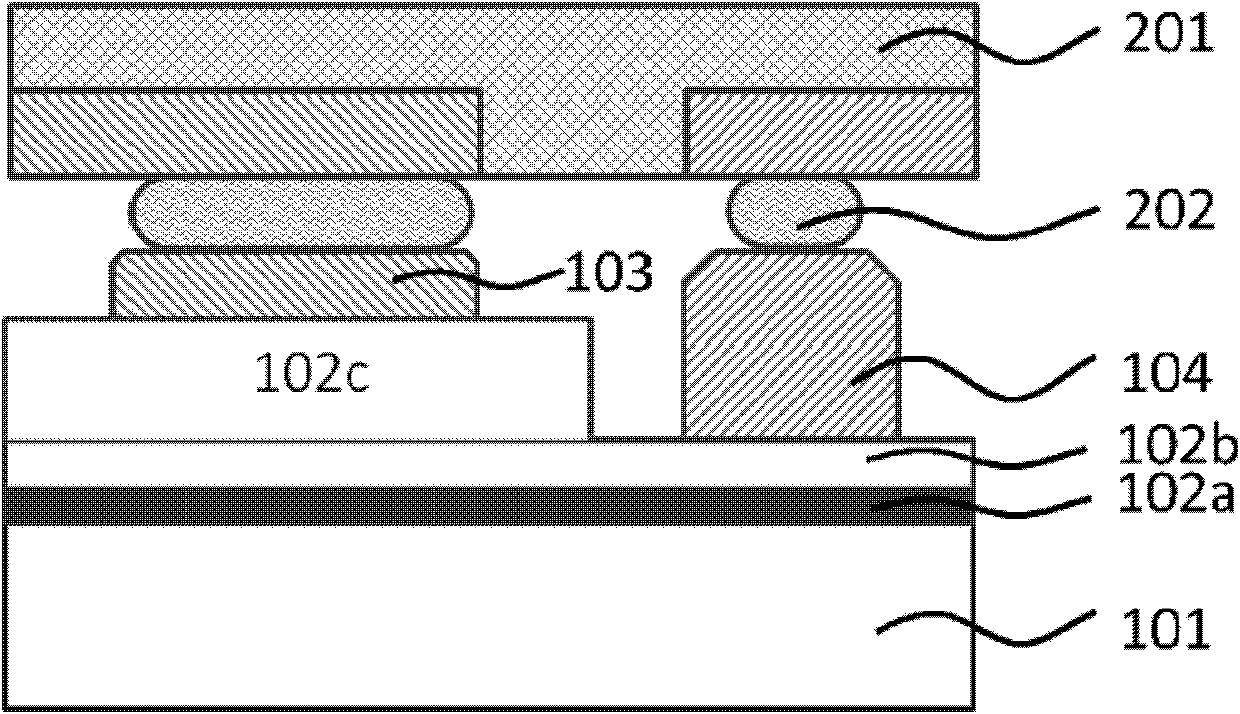
[0049] Referring to accompanying drawings 2(a)-(e), a flip-chip lateral GaN Schottky rectifier structure supported by a metal substrate and its preparation method, the steps are as follows:
[0050] Step 1: As shown in FIG. 2(a), grow the epitaxial layer of the GaN Schottky rectifier wafer on the sapphire substrate 101. The epitaxial layer includes at least from bottom to top: buffer layer 102a, heavily doped GaN ohmic The contact layer 102b and the lightly doped gallium nitride voltage blocking layer 102c; wherein the thickness of the gallium nitride voltage blocking layer 102c is at least 1um, and the average doping concentration is less than 5×10 17 cm -3 ;
[0051]The second step: as shown in Figure 2(b), the lateral structure Schottky rectifier wafer is manufactured by semiconductor micromachining technology. The main process includes: firstly, the mesa is formed by plasma dry etching method, and the The part of the contact electrode exposes the heavily doped gallium ni...
Embodiment 2
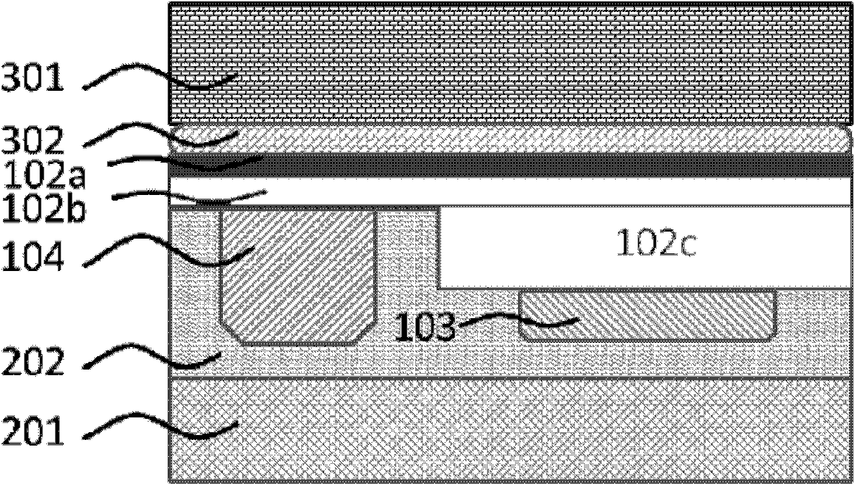
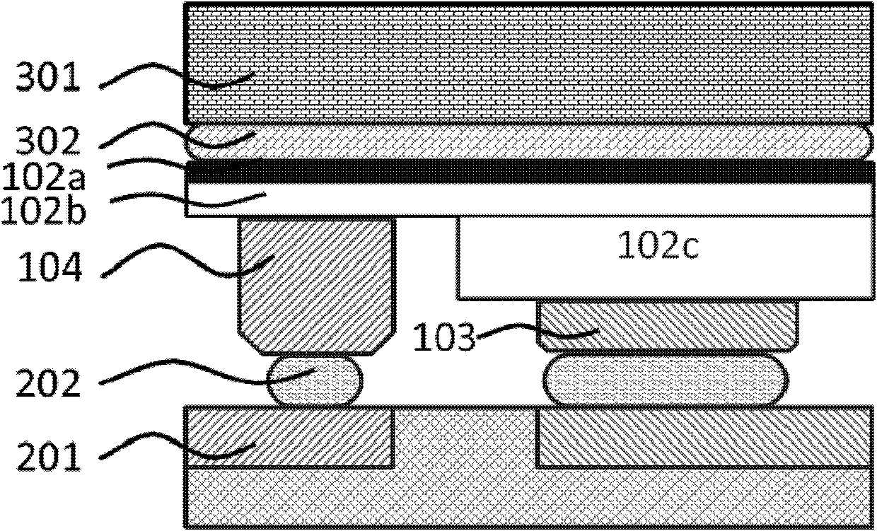
[0057] Referring to accompanying drawings 3(a)-(f), a lateral structure GaN Schottky rectifier device supported by a metal substrate and its preparation method, the steps are as follows:
[0058] Step 1: As shown in FIG. 3(a), grow a GaN Schottky rectifier epitaxial layer on a sapphire substrate 101. The epitaxial layer at least includes: a buffer layer 102a, a heavily doped gallium nitride ohmic contact layer from bottom to top 102b and the lightly doped gallium nitride voltage blocking layer 102c; wherein the thickness of the medium gallium nitride voltage blocking layer 102c needs to be at least 1um, and the average doping concentration is less than 5×10 17 cm -3 ;
[0059] The second step: as shown in Figure 3(b), the lateral structure Schottky rectifier wafer is manufactured using semiconductor micromachining technology. The main process includes: firstly, the mesa is formed by plasma dry etching method, and the epitaxial structure is exposed. Moderately heavily doped G...
PUM
| Property | Measurement | Unit |
|---|---|---|
| Thickness | aaaaa | aaaaa |
| Thickness | aaaaa | aaaaa |
| Thickness | aaaaa | aaaaa |
Abstract
Description
Claims
Application Information
 - R&D
- Intellectual Property
- Life Sciences
- Materials
- Tech Scout
- Unparalleled Data Quality
- Higher Quality Content
- 60% Fewer Hallucinations
Browse by: Latest US Patents, China's latest patents, Technical Efficacy Thesaurus, Application Domain, Technology Topic, Popular Technical Reports.
© 2025 PatSnap. All rights reserved.Legal|Privacy policy|Modern Slavery Act Transparency Statement|Sitemap|About US| Contact US: help@patsnap.com