

Modeling method of phase shift mask in photolithographic process
A modeling method and lithography technology, applied in the photolithography process of the pattern surface, the original for photomechanical processing, optics, etc., can solve the problems of restricting practical application, modeling, and increasing computational complexity, etc. Achieve the effects of avoiding computational complexity and errors, improving lithography resolution, and shortening modeling time
- Summary
- Abstract
- Description
- Claims
- Application Information
AI Technical Summary
Problems solved by technology
Method used
Image

Examples
Embodiment 1
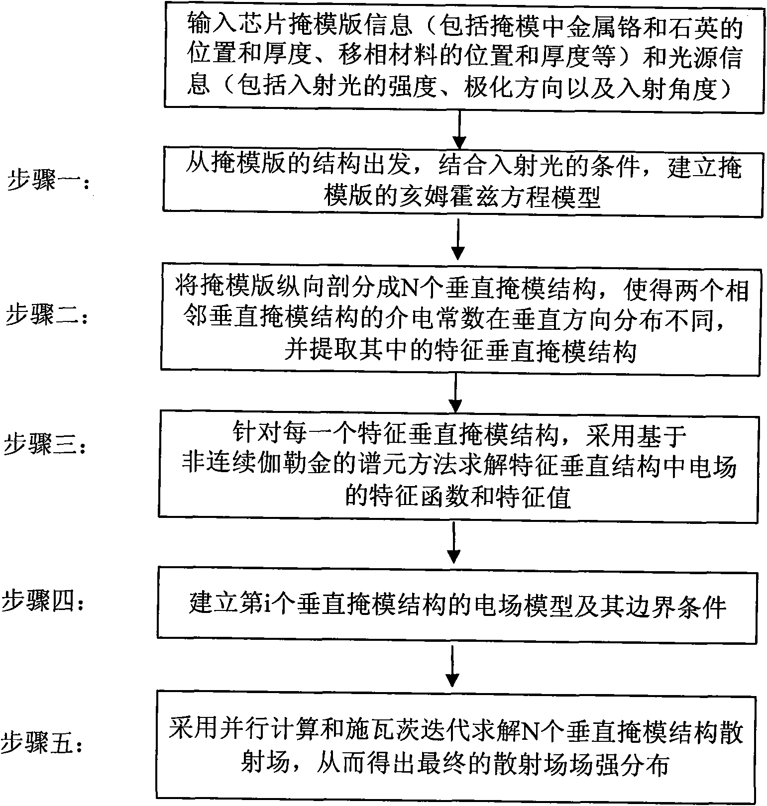
[0030] step 1
[0031] Building a Helmholtz Equation Model for Photolithographic Masks
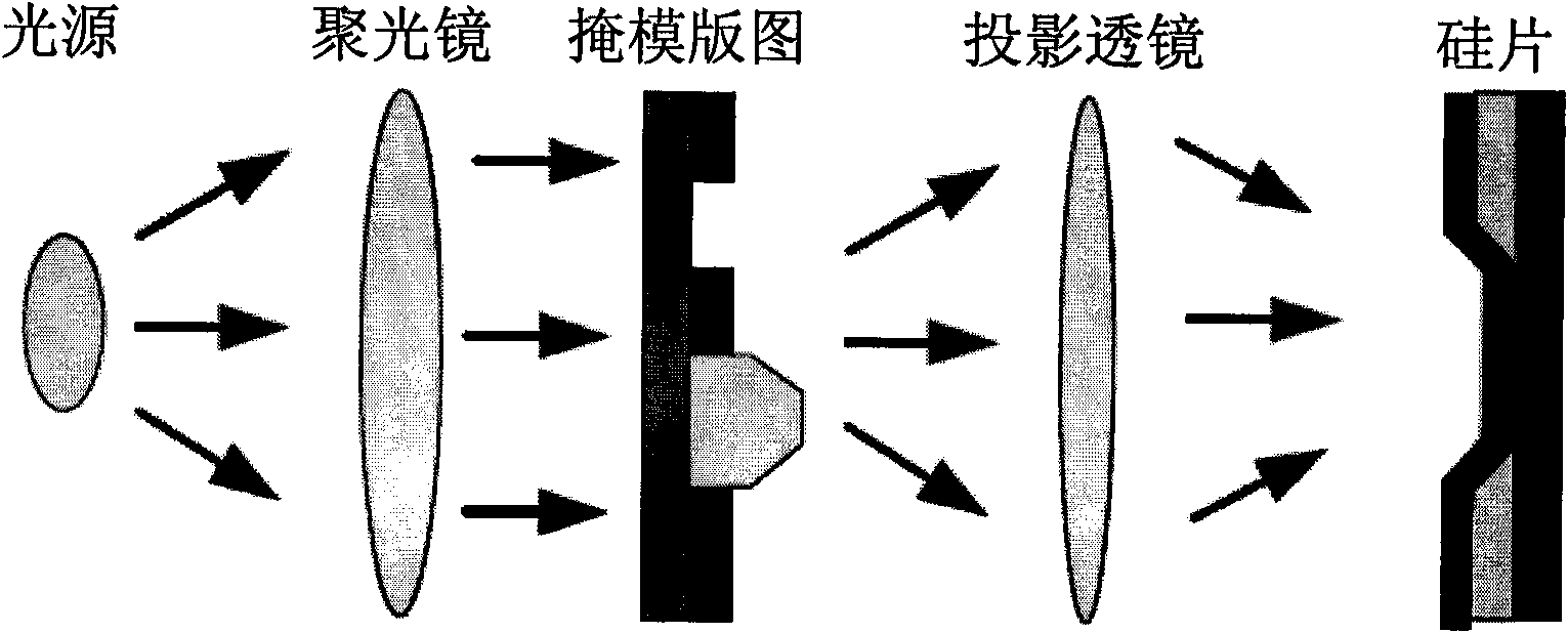
[0032] The photolithographic reticle in this embodiment is a reticle with a two-dimensional structure (such as Figure 4 shown), where the dielectric constants of all materials are uniform along the Y direction, and the incident, scattered and transmitted waves are all in the X-Z plane. Consider a TM polarized wave whose electric field component has only the Y direction The electromagnetic propagation problem of light passing through this two-dimensional reticle can be modeled by the following Helmholtz equation
[0033] ∂ ∂ x ( 1 μ ∂ E y ∂ x ) + ∂ ∂ z ...
Embodiment 3
[0077] Comparison between the light intensity distribution results obtained by the model of the present invention and the traditional waveguide method results. Considering that the waveguide method can only solve small-scale problems, a small-scale reticle with 9 vertical mask structures is selected in this embodiment, and the width of each vertical structure is 180 nm. The settings of the above parameters are not limited by the above specific embodiments.
[0078] Figure 6 It is a comparison between the light intensity distribution obtained by the model of the present invention and the light intensity distribution obtained by the traditional waveguide method. As can be seen from the figure, for the small-scale reticle, the accuracy of the light intensity distribution results obtained by the model of the present invention is equivalent to that of the results of the traditional waveguide method, which shows that the model proposed by the present invention is correct and has a...
Embodiment 4
[0080] This embodiment is the result of parallel modeling of a large-scale reticle. In this example, six reticles are selected, the width of each vertical mask structure of the reticle is still 180nm, the number of vertical mask structures ranges from 1000 to 50000, and the number of computing nodes is selected from 1 to 20. Table 1 is a comparison of the modeling time of these six reticles under 1 to 20 computing nodes using the present invention. It can be seen from the experimental results that the method of the present invention has shown good parallel characteristics to the modeling problem of large-scale reticles, and the speedup ratio (the ratio of the computing time on a single node to the parallel computing time on M computing nodes) and The number of calculation nodes is almost linear, while traditional modeling methods (such as waveguide method, finite time difference method, finite element method, etc.) cannot obtain modeling results due to high computational comp...
PUM
 Abstract
Description
Claims
Application Information