
Digital variable gain amplifier

A gain amplifier and amplifier technology, used in differential amplifiers, DC-coupled DC amplifiers, gain control and other directions, can solve the problems of low gain control accuracy, deterioration of noise performance, large chip interview, etc., to achieve high gain control accuracy, circuit The effect of reduced area and novel ideas

Inactive Publication Date: 2011-01-19
SOUTHEAST UNIV
View PDF2 Cites 26 Cited by
  • Summary
  • Abstract
  • Description
  • Claims
  • Application Information

AI Technical Summary

Problems solved by technology

However, the digital variable gain amplifier with a closed-loop structure also brings many problems: firstly, the area of ​​the voltage operational amplifier is large; based on the voltage operational amplifier, after changing the feedback network, the change of the feedback factor will lead to the change of the bandwidth, that is, the larger the gain , the smaller the bandwidth; using a current-mode operational amplifier, although it can ensure that the bandwidth basically does not change with the gain, the power consumption is too large; in addition, using a resistor feedback network, the chip is very large, and the noise performance will also deteriorate; using switched capacitors The feedback network has a complex structure, a large chip area, and requires discrete time analysis, causing certain difficulties
However, since the gain of this circuit structure is the product of the differential input transconductance and the output resistance, and the differential input transconductance is easily changed by process and other factors, and the resistance value of the resistor is also easily changed by process changes, so the gain control accuracy is not high. Linearity degree is also lower

Method used


Image

  • Digital variable gain amplifier
  • Digital variable gain amplifier
  • Digital variable gain amplifier

Examples


Embodiment Construction

[0022] The present invention will be further described below in conjunction with the accompanying drawings.

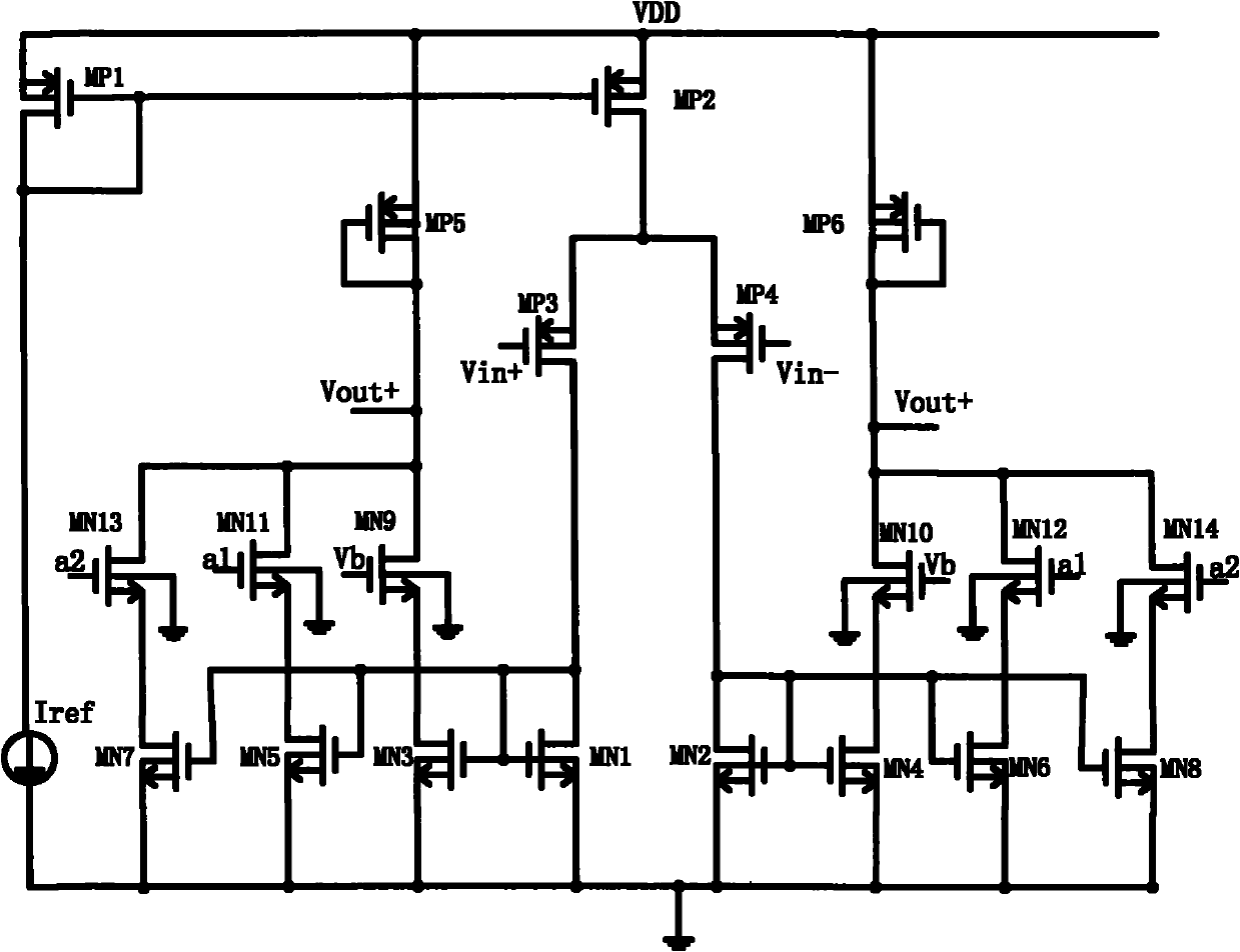
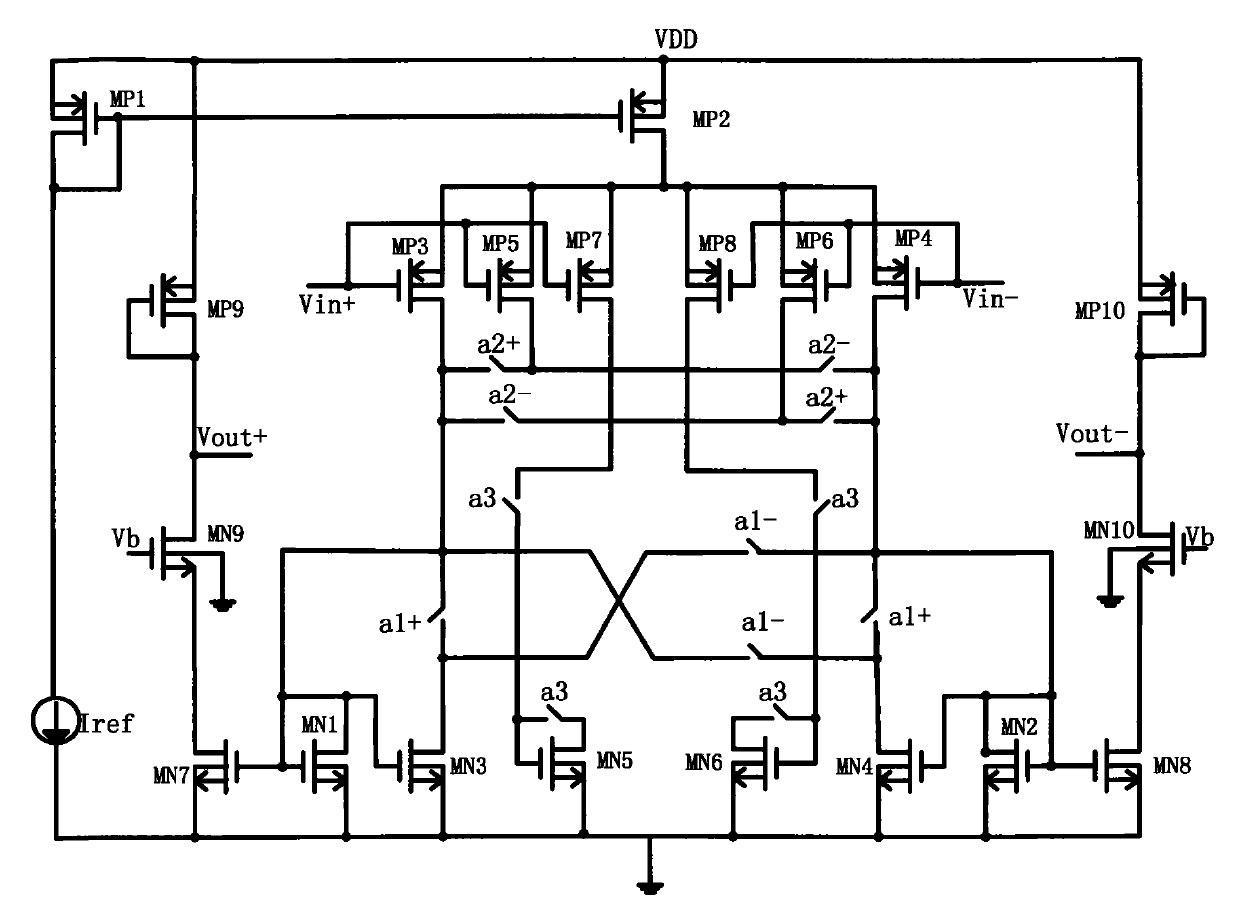
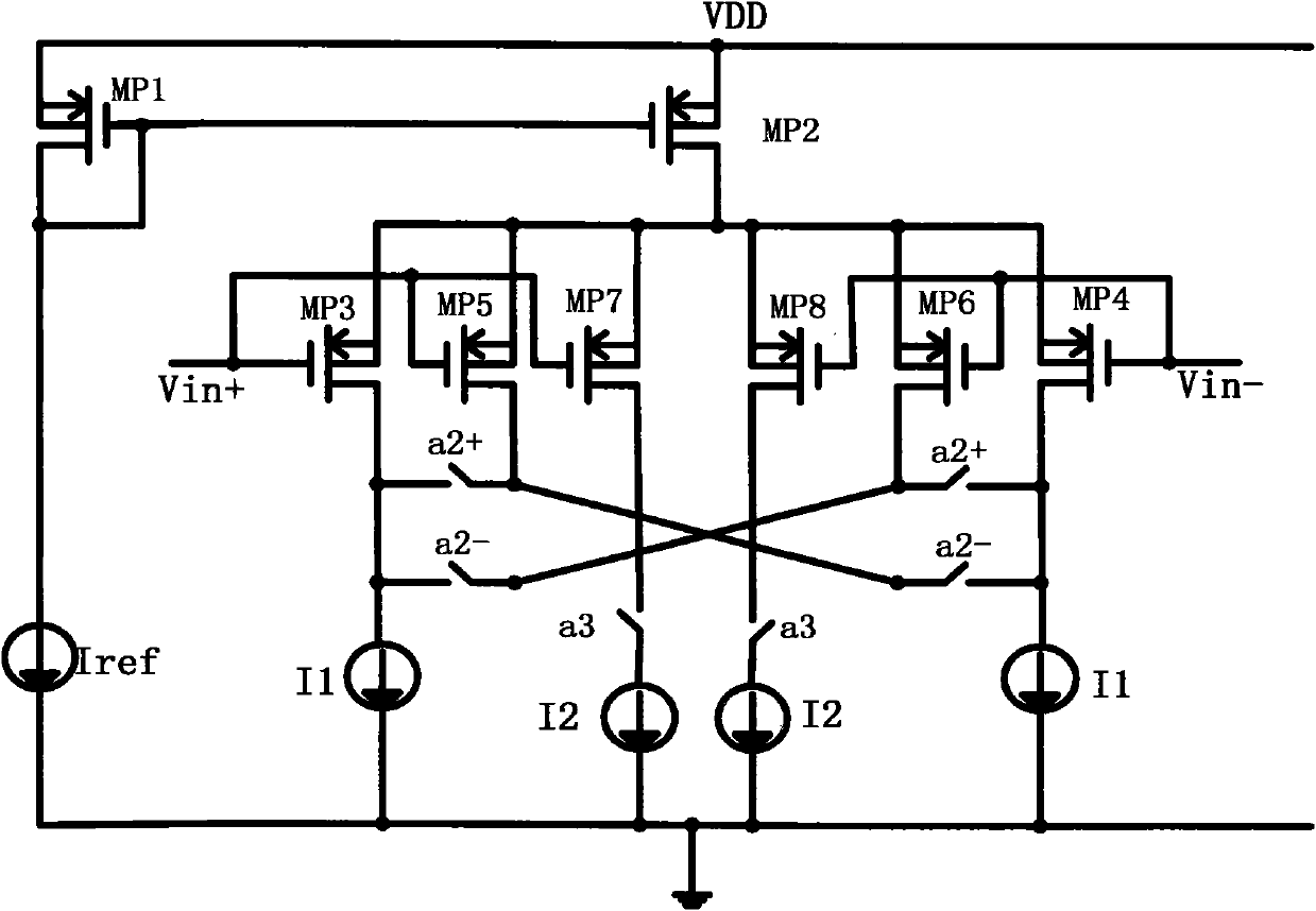
[0023] Such as figure 1 , figure 2 with image 3 As shown, it is a schematic diagram of the structure of a digital variable gain amplifier, which uses the MOS transistor differential input switch control network and the MOS transistor diode positive and negative feedback switch control network to change the proportional amplification factor of the equivalent input transconductance and the current mirror , so as to realize the digital variable gain amplification function. The digital variable gain amplifier mainly includes a differential input stage transconductance control network, a MOS transistor diode positive / negative feedback control network, and an output load stage. Three parts:

[0024] The differential input stage transconductance control network includes a bias current source Iref, a diode-connected first PMOS transistor MP1 and a second PMOS transistor MP...


PUM


Abstract

The invention discloses a digital variable gain amplifier, which utilizes a differential input end switch of an MOS (Metal Oxide Semiconductor) transistor and an MOS transistor diode positive / negative feedback switch to control the network and change equivalent input transconductance and the scale amplification factor of a current mirror so as to realize the function of digital variable gain amplification. The digital variable gain amplifier mainly comprises three parts of a differential input stage transconductance control network, a diode positive / negative feedback control network of the MOS transistor and an output load stage. The invention has the characteristics of stable direct current working point, less chip area, high gain control precision, large and relatively stable broadband,flexible gain control mode, novel thinking, simple circuit structure and the like corresponding to the traditional digital variable gain amplifier.

Description

technical field [0001] The invention relates to a digital variable gain amplifier. Background technique [0002] As the key module of radio frequency receiver, variable gain amplifier has been a research hotspot in the research of radio frequency and analog integrated circuits. A variable gain amplifier requires a trade-off between performances such as gain control range, gain control accuracy, bandwidth, linearity, area, and power consumption. In order to have the same transient response and accurately defined settling time of the automatic gain control loop (AGC) under different signal powers, the variable gain amplifier must satisfy the change of the gain relative to the change of the control signal in dB. Variable gain amplifiers are mainly classified into analog variable gain amplifiers (VGA) and digital variable gain amplifiers (PGA). However, the digital control method of the digital variable gain amplifier is easy to realize, the gain control precision is high, and...

Claims


Application Information

Patent Timeline
IPC IPC(8): H03G3/20H03F3/45
Inventor 吴建辉胡超陈超吉新村徐震竺磊徐毅杨世铎孙杰
Owner SOUTHEAST UNIV
Learn More