Manufacture method of solid insulating circuit device
A circuit device, solid insulation technology, applied in conductor/cable insulation, circuits, insulators, etc., can solve the problem that the manufacturing process parameters of epoxy resin material components are not disclosed, the material composition of conductive silicone rubber layer is not disclosed, and electrical conductivity cannot be guaranteed. Silicon rubber layer bonding strength and other issues, to achieve good bonding strength, prevent accidental electric shock, and good bonding effect
- Summary
- Abstract
- Description
- Claims
- Application Information
AI Technical Summary
Problems solved by technology
Method used
Image

Examples
Embodiment 1
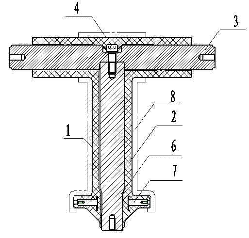
[0020] Embodiment 1: the manufacturing method of solid insulated bus bar, finished product such as figure 1 shown.
[0021] The first step: spray the processed conductor 3 and conductor 6. The sandblasting part is the part in the figure except that the two ends of the conductor 3 are used as plugs and the lower end of the conductor 6, and then remove Oil treatment, washing off the oil stains on the conductor 3 and conductor 6 during processing with detergent, and then fastening the conductor 3 and conductor 6 with bolts 4;
[0022] The second step: on the outside of the assembled conductor 3 and conductor 6, coat a layer of carbon black particles with a thickness of 0.5±0.1 mm and a weight ratio of about 10% with a particle size of 5-10 μm, 0.2% titanic acid Semi-conductive coating layer 1 composed of ester, 60% resin varnish binder, 24% xylene and 6% butanol, and then placed in an incubator at 120±5°C for preheating and curing for 40 minutes to make the conductor 3 and the ...
Embodiment 2
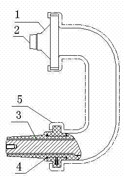
[0027] Embodiment 2: the manufacturing method of high-voltage outlet bushing, finished product such as figure 2 , image 3 shown
[0028] The first step: Spray the processed conductor 2, the sandblasting part is the part except that the two ends of the conductor 2 are made into plugs in the figure, and then perform degreasing treatment, and wash away the conductor 2 with detergent. sticky oil stains;
[0029] Step 2: Coat a layer of carbon black particles with a particle size of 5-10 μm and 0.2% titanate with a thickness of 0.5±0.1 mm on the outer surface of the conductor 2 except for the two ends. , 60% resin varnish adhesive, 24% xylene and 6% butanol to form a semi-conductive coating layer 3, and then put it into an incubator with a temperature of 125±10°C for preheating and curing for 25 minutes to make the conductor 2 The internal and external temperature is uniform, and the semi-conductive coating layer 3 is dried and cured;
[0030] Step 3: Put the preheated and cu...
Embodiment 3
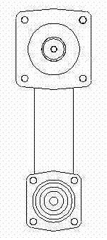
[0034] Embodiment 3: the manufacturing method of circuit breaker pole, finished product such as Figure 4 shown.
[0035] The first step: Spray the processed conductive terminal 2. The sandblasting part is the part except the upper inner hole wall and the middle inner hole wall of the conductive terminal 2 in the figure, and then carry out degreasing treatment and wash with detergent. Remove the oil stains on the conductive terminal 2 during processing;
[0036] Step 2: Coat the outer surface of the conductive terminal 2 with a thickness of 0.5±0.1 mm, which is about 10% by weight of carbon black particles with a particle size of 5-10 μm, 0.2% titanate, and 60% resin varnish Adhesive, 24% xylene and 6% butanol are mixed to form a semiconductive coating layer 3, and then placed in an incubator with a temperature of 120±5°C for preheating and curing for 40 minutes to dry and solidify the semiconductive coating layer;
[0037] Step 3: Pre-install the conductive terminal 2 and t...
PUM
| Property | Measurement | Unit |
|---|---|---|
| particle diameter | aaaaa | aaaaa |
| thickness | aaaaa | aaaaa |
| particle diameter | aaaaa | aaaaa |
Abstract
Description
Claims
Application Information
 - R&D
- Intellectual Property
- Life Sciences
- Materials
- Tech Scout
- Unparalleled Data Quality
- Higher Quality Content
- 60% Fewer Hallucinations
Browse by: Latest US Patents, China's latest patents, Technical Efficacy Thesaurus, Application Domain, Technology Topic, Popular Technical Reports.
© 2025 PatSnap. All rights reserved.Legal|Privacy policy|Modern Slavery Act Transparency Statement|Sitemap|About US| Contact US: help@patsnap.com