Silicon wafer back metallization structure and manufacturing process thereof

A technology of backside metallization and silicon wafers, which is applied in semiconductor/solid-state device manufacturing, electrical components, electric solid-state devices, etc., can solve the problem of poor coordination of subsequent packaging processes, failure to achieve low-cost stability, and existence of warping or debris And other problems, to achieve good conductivity, good adhesion, improve the effect of yield

Inactive Publication Date: 2020-02-11
NANJING INST OF PROD QUALITY INSPECTION
View PDF5 Cites 2 Cited by
  • Summary
  • Abstract
  • Description
  • Claims
  • Application Information

AI Technical Summary

Problems solved by technology

The existing structure and process can not meet the comprehensive requirements of low cost, high stability, high reliability and good cooperation with the subsequent packaging process. low level problem

Method used


Image

  • Silicon wafer back metallization structure and manufacturing process thereof
  • Silicon wafer back metallization structure and manufacturing process thereof
  • Silicon wafer back metallization structure and manufacturing process thereof

Examples


Embodiment 1

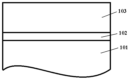
[0024] The metallization structure on the backside of the silicon wafer is as figure 1 shown. The first metal layer 102 is hafnium with a thickness of 300 nm, and the second metal layer 103 is gold with a thickness of 2000 nm. The processing steps are: front protection, back thinning, back polishing, cleaning, magnetron sputtering at a rate of 5 nm / s to prepare a hafnium layer, and evaporation at a rate of 3 nm / s to prepare a gold layer.

Embodiment 2

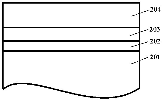
[0026] The metallization structure on the backside of the silicon wafer is as figure 2 shown. The first metal layer 202 is hafnium with a thickness of 30 nm, the second metal layer 203 is nickel with a thickness of 600 nm, and the third metal layer 204 is silver or gold with a thickness of 2000 nm. The processing steps are: front protection, back thinning, back polishing, cleaning, electron beam evaporation at a rate of 0.5 nm / s to prepare a hafnium layer, magnetron sputtering at a rate of 15 nm / s to prepare a nickel layer, and a rate of 10 nm / s to prepare a hafnium layer. nm / s rate for magnetron sputtering to prepare gold layer or 15 nm / s rate for magnetron sputtering to prepare silver layer.

Embodiment 3

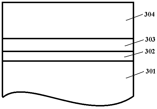
[0028] The metallization structure on the backside of the silicon wafer is as image 3 shown. The first metal layer 302 is hafnium with a thickness of 200nm, the second metal layer 303 is a gold-germanium alloy with a thickness of 500nm, and the third metal layer 304 is silver or gold with a thickness of 100nm. The processing steps are: front protection, back thinning, back polishing, cleaning, magnetron sputtering at a rate of 15 nm / s to prepare a hafnium layer, evaporation at a rate of 0.5 nm / s to prepare a gold germanium layer, and a rate of 0.5 nm / s to prepare a gold germanium layer. / s to prepare a gold layer or evaporate at a rate of 3 nm / s to prepare a silver layer.


PUM

PropertyMeasurementUnit
thicknessaaaaaaaaaa
thicknessaaaaaaaaaa
thicknessaaaaaaaaaa

Abstract

The invention belongs to the semiconductor device and integrated circuit process technology field, and especially relates to a silicon device back metallization structure and process. In the structure, at least first metal layer hafnium is deposited on a surface of a back substrate silicon wafer, and then other layers are deposited. The process comprises process steps of front surface protection,back surface thinning, back surface polishing, cleaning, physical vapor deposition and the like. By using a characteristic that hafnium and silicon form ohmic contact, a layer of hafnium is prepared on the back surface of the silicon wafer so that a lower contact resistance and better adhesion are possessed, and simultaneously good electrical conductivity, good thermal conductivity and a proper thermal expansion coefficient are achieved. A yield in a manufacturing process of a silicon device and reliability in use are effectively improved.

Description

technical field [0001] The invention belongs to the technical field of semiconductor devices and integrated circuit technology, and in particular relates to the back metallization structure and technology of silicon devices. Background technique [0002] With the development of large-scale and ultra-large-scale integrated circuits, the feature size of chips is getting smaller and higher, and the integration level is getting higher and higher. Electronic systems and complete machines are constantly developing towards miniaturization, high performance, high density, and high reliability. This puts forward higher requirements for chip interconnection materials, component soldering materials, and packaging materials. [0003] The backside metallization system is an important part of the transistor. It has two main functions, one is a larger current path, and the other is a path to transfer and dissipate the large amount of heat generated by the collector of the transistor. The...

Claims


Application Information

Patent Timeline
Patent Type & Authority Applications(China)
IPC IPC(8): H01L23/482H01L21/60
CPCH01L23/4827H01L24/03H01L2224/0345H01L2924/01072
Inventor 高瑞峰周骏贵
Owner NANJING INST OF PROD QUALITY INSPECTION
Why Eureka
Try Eureka