Cantilever beam acceleration transducer manufactured by micro-machining on single side of single silicon chip and method

An acceleration sensor and cantilever beam technology, applied in the direction of acceleration measurement using inertial force, technology for producing decorative surface effects, microstructure technology, etc., can solve the problem of reduced working bandwidth and high-range impact resistance, insufficient sensors Large gaps and other issues, to avoid spurious signal interference, reduce production costs, and simplify the production process

Active Publication Date: 2011-02-09
SHANGHAI INST OF MICROSYSTEM & INFORMATION TECH CHINESE ACAD OF SCI
View PDF5 Cites 32 Cited by
  • Summary
  • Abstract
  • Description
  • Claims
  • Application Information

AI Technical Summary

Problems solved by technology

This type of acceleration sensor mainly has the following two different structures: (1) cantilever beam + mass block structure, for example, [1] Y Ning, Y Loke, G Mckinnon MCKNNON G, Fabrication and characterization of high-g-force, silicon piezoresistive accelerometers, Sensors and Actuators.1995, A48:55-61. (2) cantilever beam structure, for example, [2] J.Dong, X.Li, Y.Wang, D.Lu and S.Ahat, Silicon micromachined high-shock accelerometers with acurved-surface-application structure for over-rang stop protection and free-mode-resonance depression, J.Micromech.Microeng.2002, 12(6): 742-746. The surface micromachined acceleration sensor needs to spend a lot of time in the production process to use KOH solution to thin the silicon wafer in a large area and deep to the expected thickness of the structural beam, which not only prolongs the production cycle, but also (100) silicon wafe

Method used


Image

  • Cantilever beam acceleration transducer manufactured by micro-machining on single side of single silicon chip and method
  • Cantilever beam acceleration transducer manufactured by micro-machining on single side of single silicon chip and method
  • Cantilever beam acceleration transducer manufactured by micro-machining on single side of single silicon chip and method

Examples


Embodiment 1

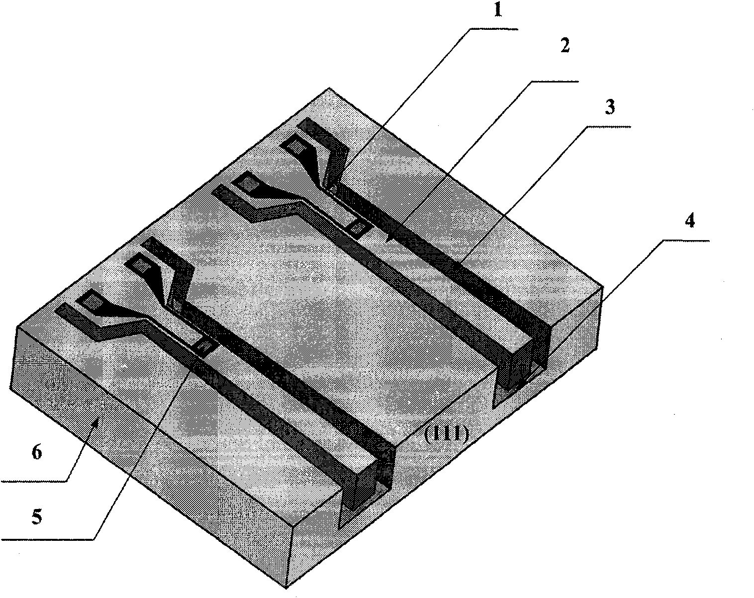
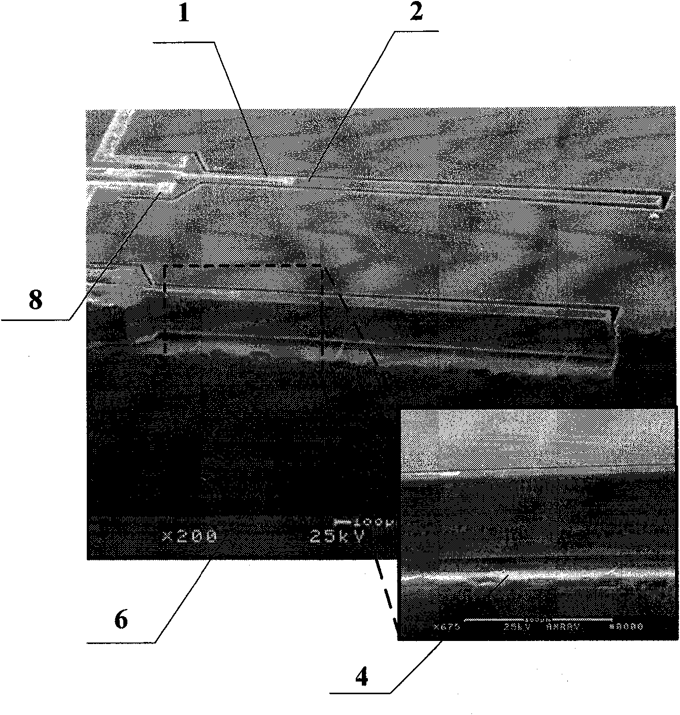
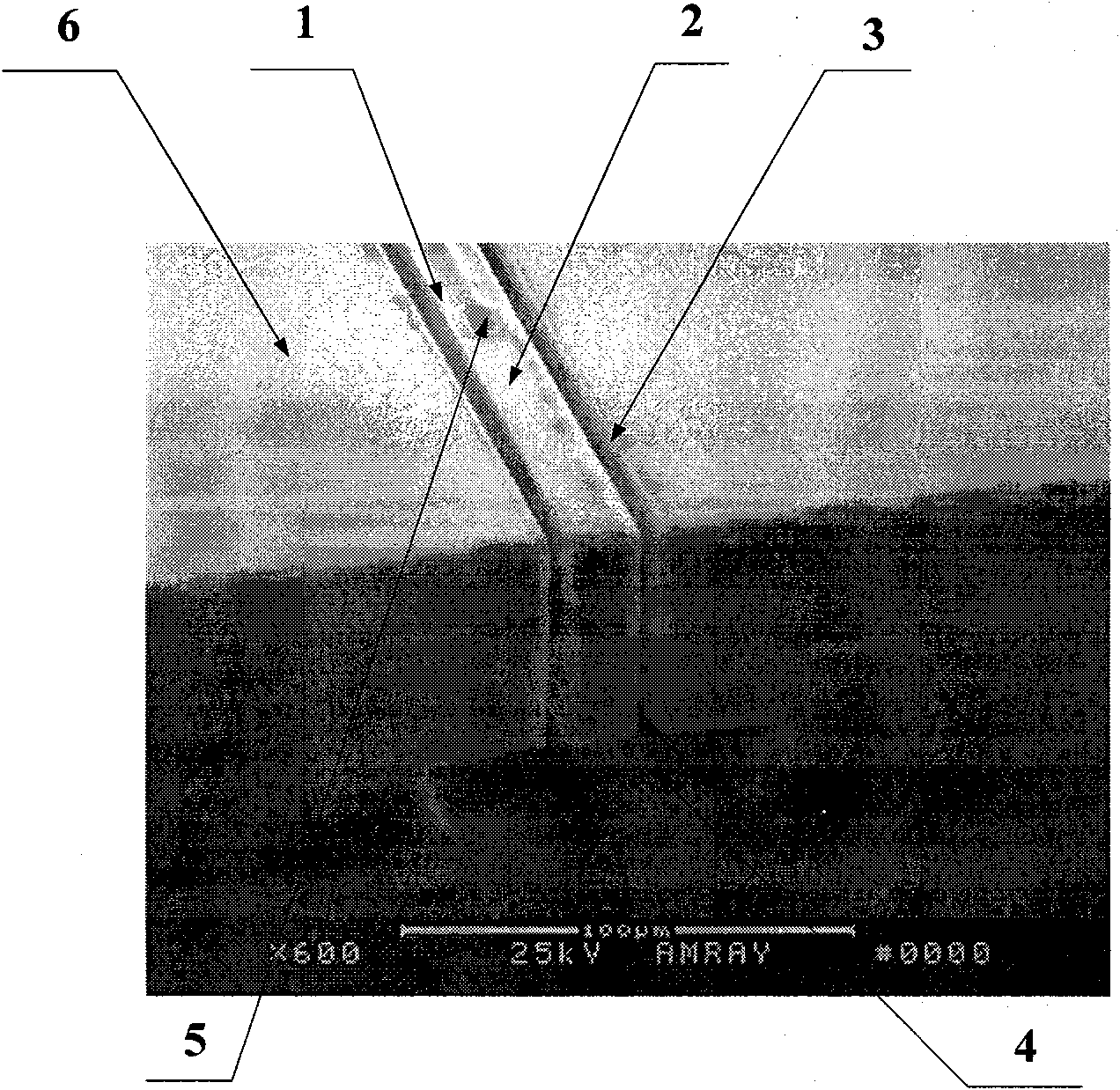
[0040] A cantilever beam accelerometer produced by single-sided microprocessing on a single silicon chip, its structure is mainly composed of a single crystal silicon substrate, a detection cantilever beam, a sensitive resistor, a high overload shock resistant curved surface, and a gap in the vertical sensitive direction. It is characterized in that the whole acceleration sensor adopts (111) single silicon chip to make (see image 3 ), different from the cantilever beam sensitive structure formed by micromachining on both sides of (100) silicon wafers in the past, the sensor of the present invention adopts a single silicon wafer integrated structure, and single-sided micromachining is performed on the front side of the silicon wafer. The sensor adopts double cantilever beam piezoresistive detection method. The cantilever beams have the same structural size and are arranged in parallel in the same direction. The anti-high overload impact surface is located on both sides of the c...

Embodiment 2

[0042] A cantilever beam accelerometer with a measuring range of 100,000 g produced by single-sided microprocessing on a single silicon chip and its manufacturing method: the designed cantilever beam structure has a length of 400 μm, a thickness of 50 μm, and a width of 18.5 μm. The overall size of the chip after processing is 1.5 μm. ×1.5×0.8mm 3 (The overall size of the traditional piezoresistive acceleration sensor after processing is 6.0×6.0×1.30mm 3 , see reference [2] for details). The entire sensor is implemented on an n-type (111) single crystal silicon chip (because when n-type piezoresistors are processed on p-type (111) single crystal silicon, the piezoresistive coefficient is relatively small, which is not conducive to improving the sensitivity of the sensor, and the n-type ( 111) Silicon chip production), the sensor is an integrated structure of a single silicon chip, and the sensitivity of the sensor is 0.35μV / g (see Figure 9 ), when the temperature ranges fro...


PUM

PropertyMeasurementUnit
Lengthaaaaaaaaaa
Thicknessaaaaaaaaaa
Widthaaaaaaaaaa

Abstract

The invention relates to a cantilever beam acceleration transducer manufactured by micro-machining on a single side of a single silicon chip and a manufacturing method. The acceleration transducer is characterized in that: an accelerometer is manufactured by micro-mechanical single side machining through the single silicon chip, so that stress caused by the bonding process of a plurality of chipsand different materials is avoided. In order to realize a single side-machined cantilever beam sensitive structure, the cantilever beam structure is released by transversely etching the bottom of thecantilever beam by an anisotropic corrosion method after deep structural etching. The structure provides air squeeze-film damping and mechanical overload protection in a sensitive direction, solves the problem of the absence of air squeeze-film damping in the vertical sensitive direction of the conventional structure and prevents parasitic signal interference caused by structural resonance in thevertical direction. The acceleration transducer has the characteristics of particular suitability for measuring a high g value, simple structure, small size of the chip and the like. Simultaneously, a single side process can use low-cost single throwing silicon chips, is suitable for low-cost mass manufacturing and has higher performance and wide application prospects.

Description

technical field [0001] The invention relates to a cantilever beam acceleration sensor and method produced by single-sided micro-machining on a single silicon chip, belonging to the field of silicon micro-mechanical sensors. Background technique [0002] With the continuous development of MEMS technology and the maturity of silicon micromachined processing technology, silicon micromachined acceleration sensors are widely used in different fields due to their low price, high precision and suitability for mass production, such as automotive airbags and robot industries And automation control and other monitoring projects of various movements. At present, acceleration sensors for high-g range detection in high-shock environments are widely used in military, aerospace and other fields. In recent years, with the development of penetrating weapons and the continuous deepening of research on high-explosive shock phenomena, the demand and requirements for high-range acceleration sen...

Claims


Application Information

Patent Timeline
IPC IPC(8): G01P15/12B81C1/00B81B3/00
Inventor 李昕欣王家畴
Owner SHANGHAI INST OF MICROSYSTEM & INFORMATION TECH CHINESE ACAD OF SCI
Why Eureka
Try Eureka