Method for directly writing metal micro-nano structure by ultraviolet laser interferometry etching

A technology of ultraviolet laser and micro-nano structure, applied in the direction of nano-structure manufacturing, laser welding equipment, metal processing equipment, etc., can solve the problems that limit the wide application of metal photonic crystals and practical technology development, complex preparation process, expensive preparation equipment, etc. , to achieve the effect of improving adhesion and firmness, good repeatability and high preparation efficiency

Inactive Publication Date: 2011-02-16
BEIJING UNIV OF TECH
View PDF2 Cites 16 Cited by
  • Summary
  • Abstract
  • Description
  • Claims
  • Application Information

AI Technical Summary

Problems solved by technology

However, these preparation methods have problems such as complex preparation process, expensive preparation equipment, low efficiency, and high cost, which greatly limit the wide application and practical technology development of metal photonic crystals.

Method used


Image

  • Method for directly writing metal micro-nano structure by ultraviolet laser interferometry etching
  • Method for directly writing metal micro-nano structure by ultraviolet laser interferometry etching
  • Method for directly writing metal micro-nano structure by ultraviolet laser interferometry etching

Examples


Embodiment 1

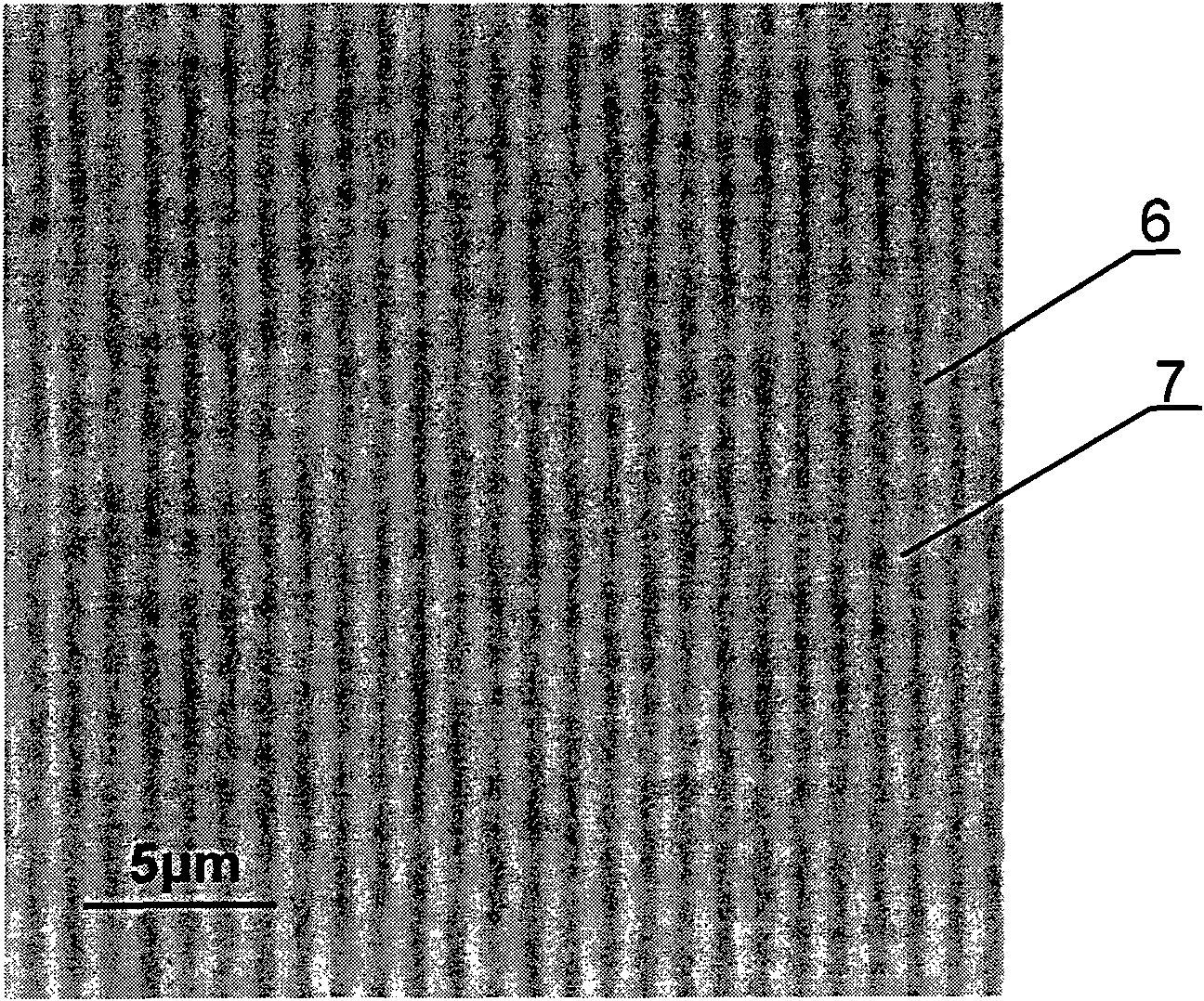
[0020] Example 1: Preparation of a one-dimensional gold nanowire photonic crystal structure.

[0021] 1) dissolving the chemically synthesized gold nanoparticles with an average diameter of 5nm in organic solvents such as toluene or xylene to make a gold nanoparticle colloid solution with a concentration of 100 mg / ml;

[0022] 2) Spin-coat the colloidal solution of gold nanoparticles on the glass substrate. The spin coating speed is 2000rpm, and the corresponding film thickness is about 200nm;

[0023] 3) The sample spin-coated with the gold nanoparticle colloidal film is placed on a heating plate, and heated at 250° C. for 25 seconds to obtain a sample with a uniform thickness and continuous gold film structure.

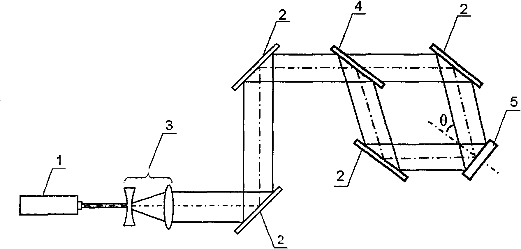
[0024] 4) Place the gold thin film sample prepared above in the interference light path, such as figure 1 As shown, the angle between the two beams is θ=7.8°. Using manual triggering to make the laser emit a laser pulse with an energy of 20mJ, a pulse width of 6n...

Embodiment 2

[0027] 1) dissolving chemically synthesized gold nanoparticles with an average diameter of 5nm in organic solvents such as toluene or xylene to make a gold nanoparticle colloid solution with a concentration of 100mg / ml;

[0028] 2) Spin-coat the colloidal solution of gold nanoparticles on the glass substrate. The spin coating speed is 2000rpm, and the corresponding film thickness is about 200nm;

[0029] 3) The sample spin-coated with the gold nanoparticle colloidal film is placed on a heating plate, and heated at 250° C. for 25 seconds to obtain a sample with a uniform thickness and continuous gold film structure.

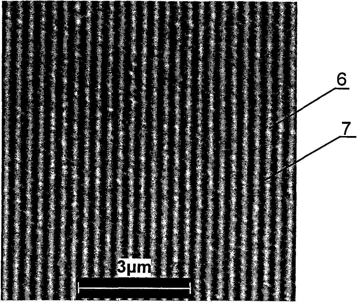
[0030] 4) Place the gold thin film sample prepared above in the interference light path, such as figure 1 As shown, the angle between the two beams of light is θ=26.3°. Using manual triggering to make the laser emit a laser pulse with an energy of 20mJ, a pulse width of 6ns, and a wavelength of 266nm, a periodic one-dimensional metal grating structure can be etc...

Embodiment 3

[0032] Example 3: Preparation of two-dimensional gold nanowire photonic crystal structure

[0033] On the basis of the one-dimensional metal nano-grating preparation technology realized in Example 1, the sample is rotated 90° around its normal, and then the second exposure and ablation are performed to realize the preparation of a two-dimensional metal nano-grating structure.


PUM

PropertyMeasurementUnit
wavelengthaaaaaaaaaa

Abstract

The invention discloses a method for directly writing a metal micro-nano structure by ultraviolet laser interferometry etching, and belongs to the technical field of nano ophoelectronic materials and devices. A metal nanoparticle colloid is synthesized chemically and then is directly acted on the surface of a metal film by a heat treatment process and an ultraviolet laser interferometry etching technique and thus, the novel technique for preparing a one-dimensional or two-dimensional photnic crystal is realized. The method has the advantages of low cost, high efficiency, capacity of preparinglarge-area metal photonic crystals, and the like.

Description

technical field [0001] The invention belongs to the technical field of nano-optoelectronic materials and devices, and relates to directly writing period-controllable metal photonic crystal structures on metal thin films by using an ultraviolet laser interference ablation method. Background technique [0002] Periodically arranged metal nanowires, metal nanocolumns or metal nanohole structures are usually called metal photonic crystals. The electromagnetic wave incident on the metal photonic crystal will cause the collective oscillation of electrons in the metal, resulting in particle plasmon resonance or localized surface plasmon resonance, which is characterized by a strong characteristic extinction spectrum in photophysics, mainly including plasmon resonance absorption and light There are two physical mechanisms for scattering. Using the coupling effect of particle plasmon resonance and the periodic structure of metal photonic crystals, new optoelectronic devices such as ...

Claims


Application Information

Patent Timeline
Patent Type & Authority Applications(China)
IPC IPC(8): B82B3/00B23K26/00B23K26/362
Inventor 张新平庞兆广刘红梅
Owner BEIJING UNIV OF TECH
Why Eureka
Try Eureka