Method for preparing copper indium gallium selenide thin film battery

A technology of copper indium gallium selenide and thin-film batteries, which is applied in the manufacture of circuits, electrical components, and final products, and can solve problems such as uneven cutting line width, a large amount of residue, debris, and short-circuiting of sub-batteries

Active Publication Date: 2011-02-23
珠海中科先进科技产业有限公司
View PDF4 Cites 15 Cited by
  • Summary
  • Abstract
  • Description
  • Claims
  • Application Information

AI Technical Summary

Problems solved by technology

[0005] However, see figure 1 , when the back electrode is cut by mechanical scribing, because the film is brittle, the width of the cutting line will be

Method used


Image

  • Method for preparing copper indium gallium selenide thin film battery
  • Method for preparing copper indium gallium selenide thin film battery
  • Method for preparing copper indium gallium selenide thin film battery

Examples


preparation example Construction

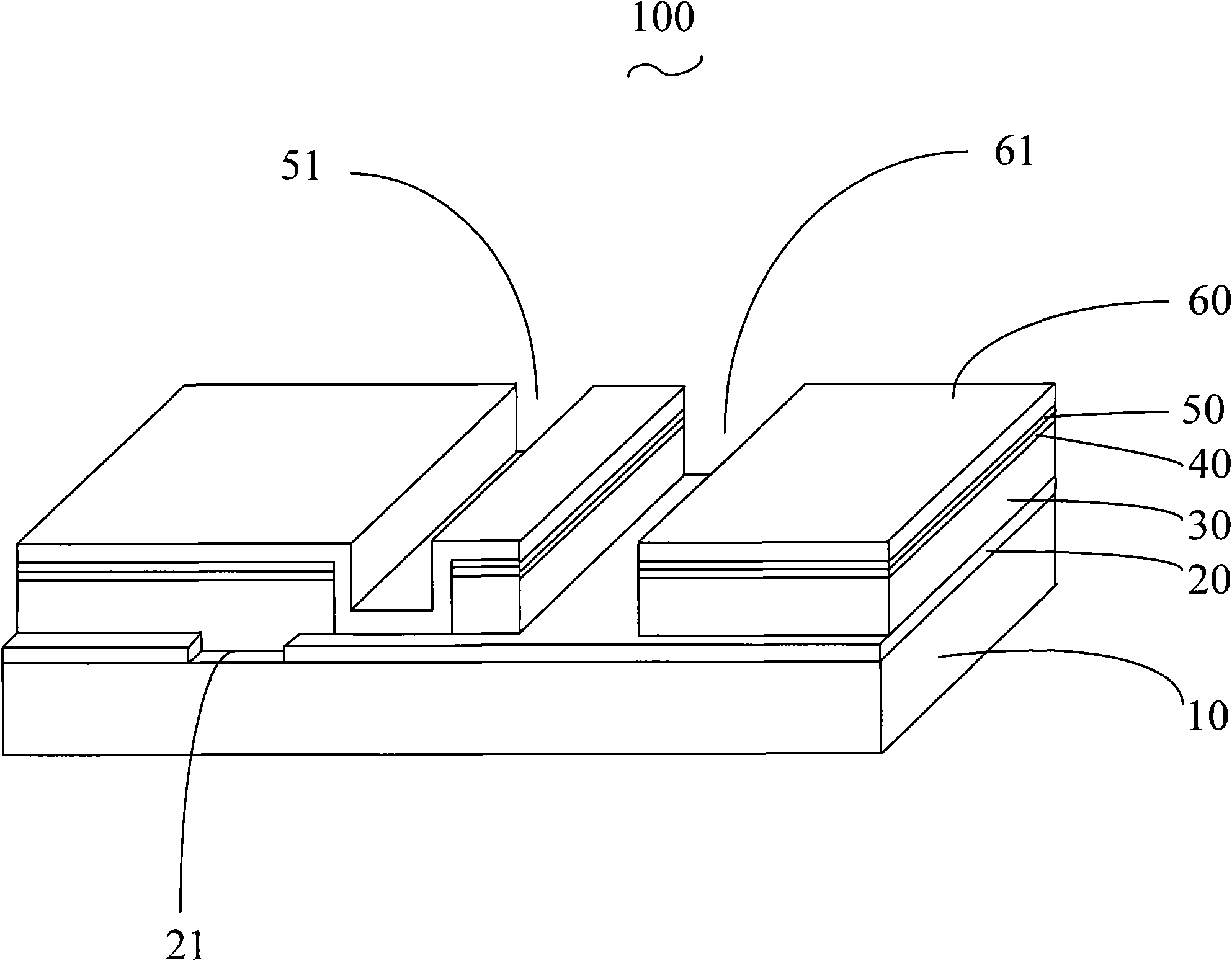
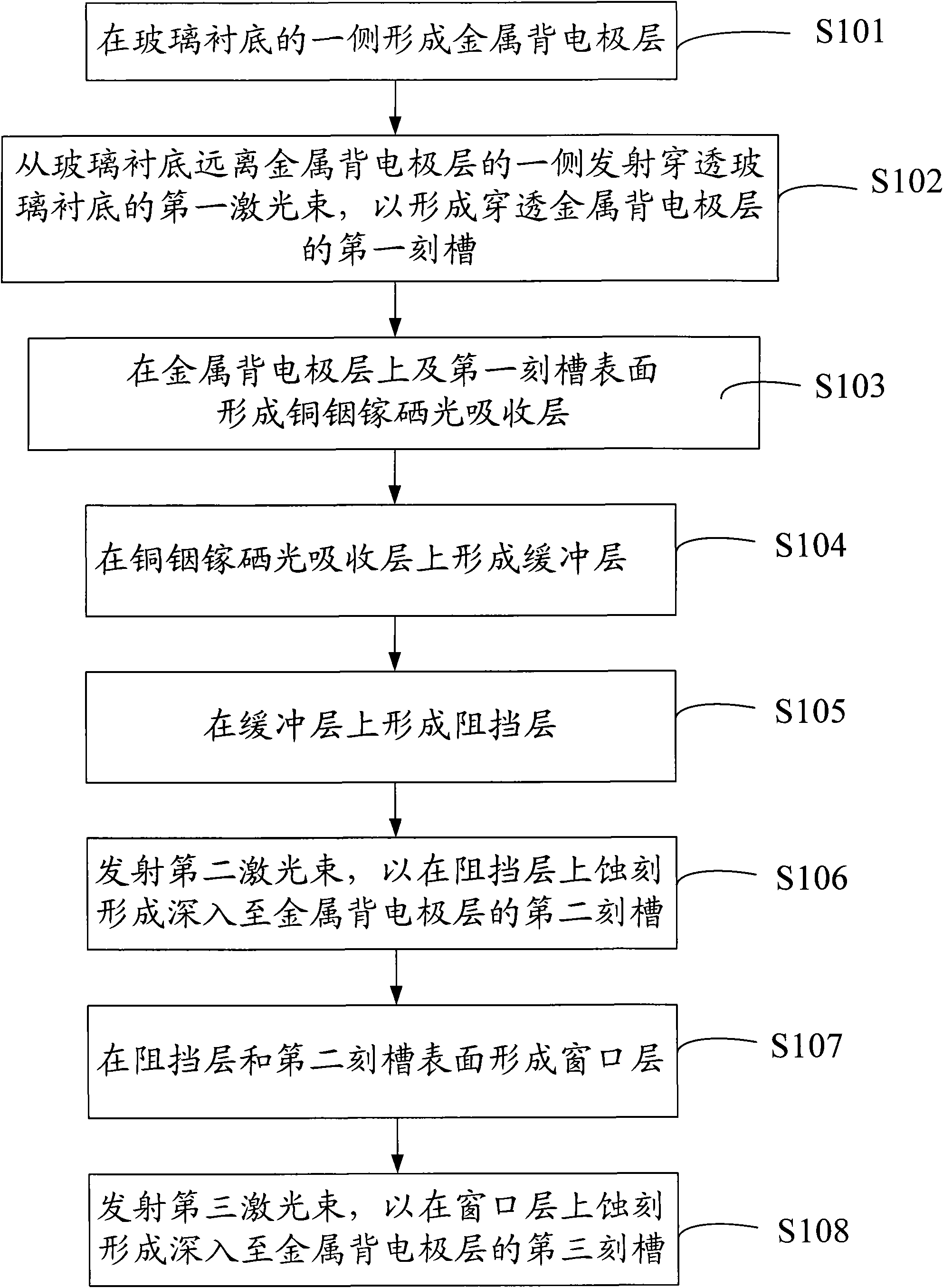
[0026] Please also refer to image 3 , the preparation method of the copper indium gallium selenide thin film battery 100 includes the following steps:

[0027] In step S101 , a flat glass substrate 10 is provided, and a metal back electrode layer 20 is formed on one side of the glass substrate 10 . Mo can be deposited on the glass substrate 10 with a thickness of about 1 μm by DC magnetron sputtering to form the metal back electrode layer 20 .

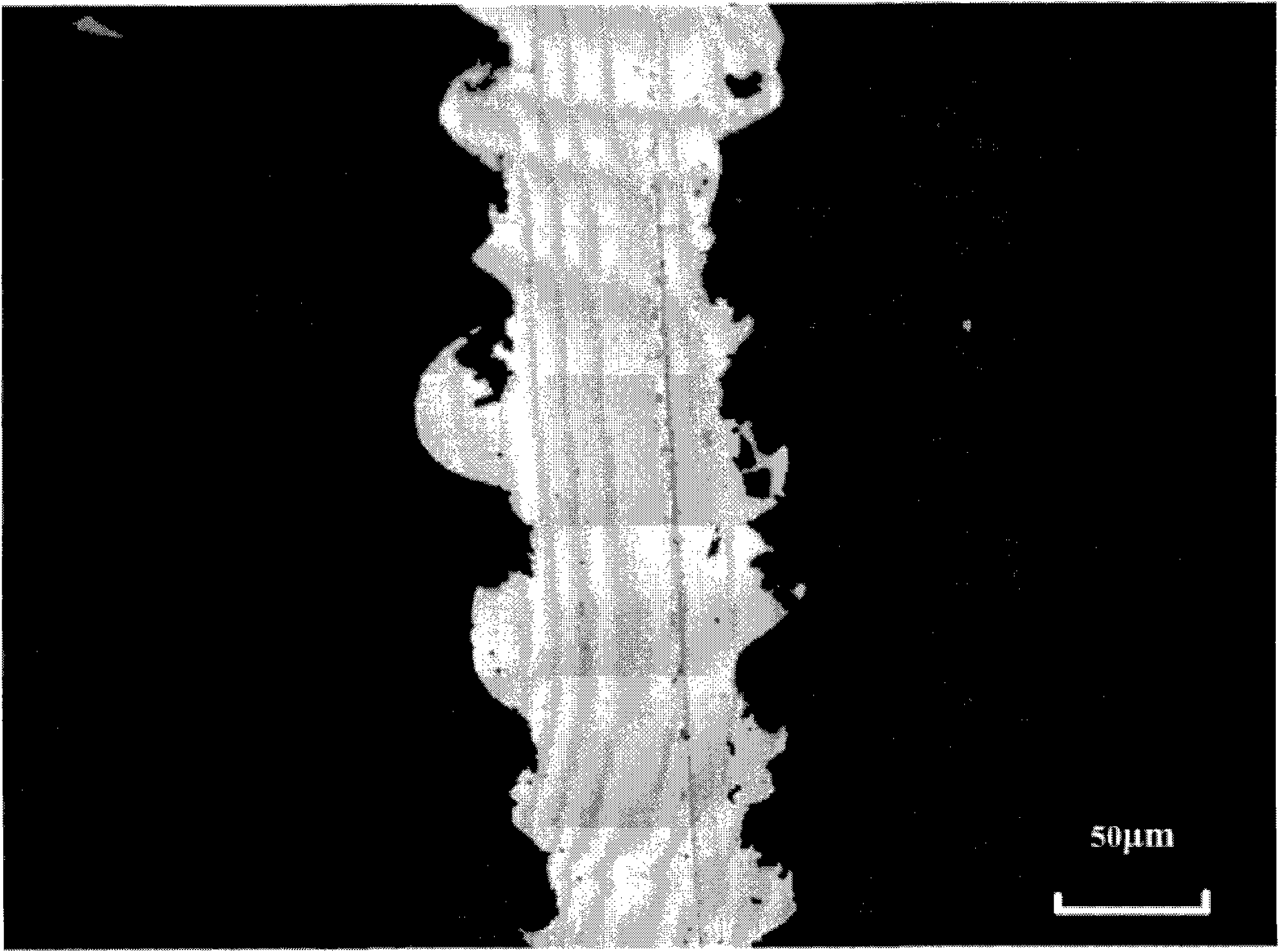
[0028] Step S102, emitting a first laser beam penetrating the glass substrate 10 from the side of the glass substrate 10 away from the metal back electrode layer 20 to form a first groove 21 penetrating the metal back electrode layer 20 to divide the cell unit, to ensure insulation between each unit. The first laser beam is preferably a pulsed laser with a wavelength range of 248-1064 nm, a scanning speed of 20-2000 mm / sec, and an adjustment frequency of 30-80 KHz. The width of the first groove 21 is not more than 60 microns. Emit...

Embodiment 1

[0037]Embodiment 1: Soda-lime glass is used as the substrate, and the thickness of the substrate is 2 mm. A molybdenum metal target is sputtered by a DC magnetron sputtering process to deposit a molybdenum metal back electrode layer with a thickness of 2 μm. A laser beam with a wavelength of 532nm is used to etch the molybdenum metal back electrode layer for the first time from the side of the glass surface, the frequency is 30KHz, the scanning speed is 800mm / sec, and the etching line width is 50 microns. After the etching is completed, put it into deionized water with a resistance of 18 megohm for ultrasonic vibration for 3 minutes, rinse with 80% ethanol solution, and blow dry with high-pressure nitrogen. The CIGS absorber layer was deposited with a magnetron sputtering followed by selenization process with a thickness of 0.5 μm. Deposit the CdS buffer layer with a chemical water bath method to a thickness of 0.05 μm. The ZnO ceramic target was sputtered by radio frequency ...

Embodiment 2

[0039] Embodiment 2: Soda-lime glass is used as the substrate, the thickness of the substrate is 2 mm, and the molybdenum metal target is sputtered by DC magnetron sputtering process to deposit the molybdenum metal back electrode layer with a thickness of 2 μm. A laser beam with a wavelength of 248nm is used to etch the molybdenum metal back electrode layer for the first time from the side of the glass surface, the frequency is 50KHz, the scanning speed is 900mm / sec, and the etching line width is 50 microns. After the etching is completed, put it into deionized water with a resistance of 18 megohm for ultrasonic vibration for 3 minutes, rinse with 80% ethanol solution, and blow dry with high-pressure nitrogen. The CIGS absorber layer was deposited with a magnetron sputtering followed by selenization process with a thickness of 0.5 μm. Deposit the CdS buffer layer with a chemical water bath method to a thickness of 0.05 μm. The ZnO ceramic target was sputtered by radio frequen...


PUM

PropertyMeasurementUnit
Widthaaaaaaaaaa
Widthaaaaaaaaaa

Abstract

The invention discloses a method for preparing a copper indium gallium selenide thin film battery, which comprises the following steps of: forming a metal back electrode layer on one side of a glass substrate; emitting a first laser beam penetrating the glass substrate from the side of the glass substrate away from the metal back electrode layer so as to form a first groove penetrating the metal back electrode layer; forming a copper indium gallium selenide light absorbing layer on the metal back electrode layer and the surface of the first groove; forming a buffer layer on the copper indium gallium selenide light absorbing layer; forming a barrier layer on the buffer layer; emitting a second laser beam to etch the barrier layer so as to form a second groove reaching the metal back electrode layer; forming a window layer on the barrier layer and the surface of the second groove; and emitting a third laser beam to etch the window layer so as to form a third groove reaching the metal back electrode layer. The copper indium gallium selenide thin film battery prepared by the method has the advantage of low possibility of generating short circuit.

Description

【Technical field】 [0001] The invention relates to a method for preparing a semiconductor device, in particular to a method for preparing a copper indium gallium selenium thin film battery. 【Background technique】 [0002] Copper Indium Gallium Selenide (Cu(In,Ga)Se 2 , referred to as CIGS) thin-film photovoltaic cells have the advantages of low cost, high efficiency, and good stability, and are recognized as the second-generation solar cells with the most development and market potential. People's research on it began in the early 1980s. After nearly 30 years of development, the theoretical research and preparation process of copper indium gallium selenium thin film solar cells have achieved gratifying results. At present, its highest laboratory photoelectric conversion efficiency has reached 21.1%, is currently the highest conversion efficiency of thin-film solar photovoltaic cells. [0003] Copper indium gallium selenide thin film solar cells are generally made by the fol...

Claims


Application Information

Patent Timeline
IPC IPC(8): H01L31/18
CPCY02P70/50
Inventor 马续航
Owner 珠海中科先进科技产业有限公司
Why Eureka
Try Eureka