Micro gas-phase chromatographic column with ultrahigh depth-to-width ratio and MEMS machining method thereof
A micro gas chromatography and aspect ratio technology, which is applied in the field of ultra-high aspect ratio micro gas chromatography column and its MEMS processing, can solve the problems of inability to process, affect production efficiency, slow dry etching etch rate, etc., and achieve improved performance , The effect of simple and easy process
- Summary
- Abstract
- Description
- Claims
- Application Information
AI Technical Summary
Problems solved by technology
Method used
Image
Examples
Embodiment 1
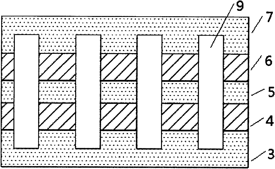
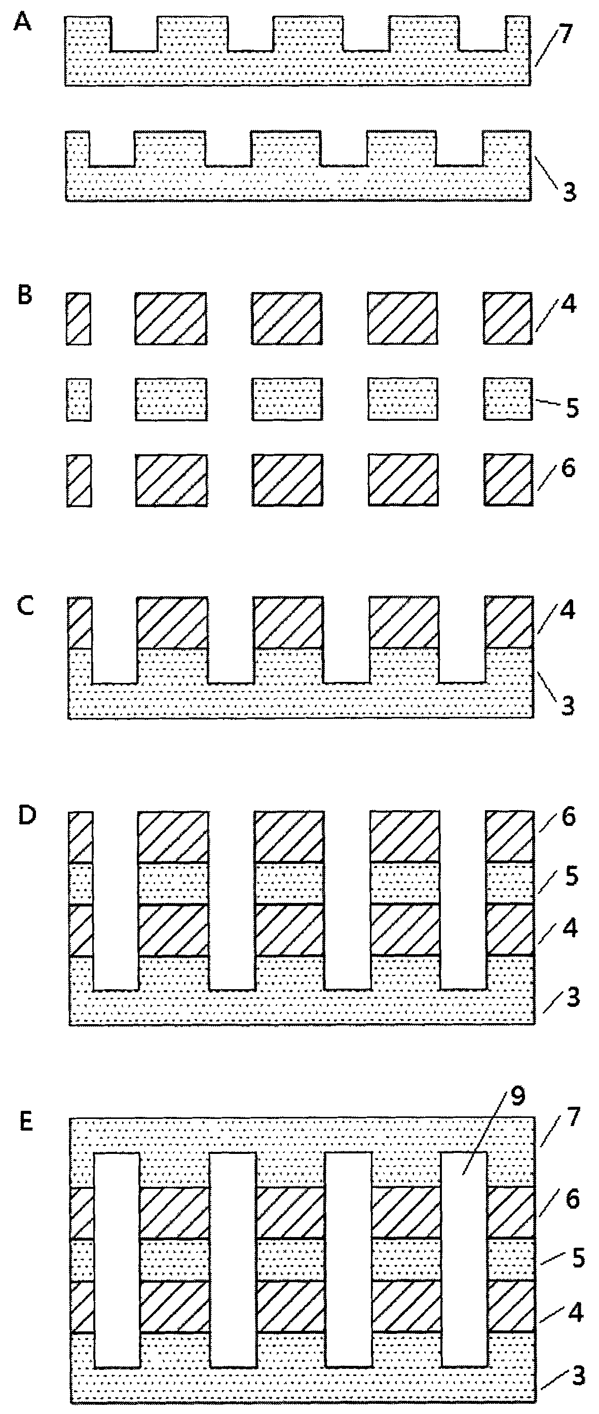
[0028] A five-layer structure of ultra-high aspect ratio spiral micro gas chromatographic column, the bottom layer is glass, the middle layer has three layers, silicon, glass and silicon in turn, and the top layer is glass, using deep reactive ion etching (DRIE dry etching) ) combined with anodic bonding technology for MEMS processing. The processing flow is as follows:
[0029] ①Design and process masks for the bottom layer and top layer respectively, and the patterns on the two masks are mirror-symmetrical as Figure 4 As shown, the width of the spiral gas path groove is 30 μm, the groove interval is 150 μm, and the length is about 50 cm.
[0030] ② Etch the Pyrex7740 glass with the bottom and top mask DRIE, the thickness of the glass is 500 μm, etch to about 250 μm, and use it as the bottom and top layer for backup;
[0031] ③Etch 360μm silicon wafer and 300μm thick Pyrex7740 glass using the underlying mask DRIE, etch through both the silicon wafer and glass, and use it a...
Embodiment 2
[0036] A five-layer structure ultra-high aspect ratio loop-shaped micro gas chromatographic column, the structure of the micro gas chromatographic column is the same as that of Example 1 except that the chromatographic gas flow channel is loop-shaped. Since the linear etching pattern itself has mirror symmetry, only one mask pattern is needed to complete the dry etching of the bottom layer, the middle layer and the top layer. The MEMS processing flow of the column is as follows:
[0037] ①Design and process as Figure 5 As shown in the mask, there are multiple loop patterns on the mask, each loop is an air channel groove, the groove width is 50 μm, the interval is 150 μm, and the total length is about 50 cm;
[0038] ②~⑤: ②~⑤ with embodiment 1;
[0039] ⑥Turn the top layer of glass over along the mirror symmetry axis of its etched pattern, so that the etched surface is upside down on the third intermediate layer, and after it is completely aligned with the pattern of the low...
PUM
| Property | Measurement | Unit |
|---|---|---|
| Thickness | aaaaa | aaaaa |
Abstract
Description
Claims
Application Information


