High-voltage low-on-resistance LDMOS device and manufacturing method thereof

A low on-resistance, high-voltage technology, used in semiconductor/solid-state device manufacturing, semiconductor devices, electrical components, etc., can solve the problems of increased chip cost, high process requirements, poor compatibility, etc., to reduce on-resistance, reduce manufacturing Cost, effect of improving electric field distribution

Inactive Publication Date: 2011-04-06
UNIV OF ELECTRONIC SCI & TECH OF CHINA
View PDF7 Cites 24 Cited by
  • Summary
  • Abstract
  • Description
  • Claims
  • Application Information

AI Technical Summary

Problems solved by technology

The SINGLE/DOUBLE-RESURF LDMOS devices in the prior art all use a single well process to manufacture the N-well region 16, which is the drift region of the LDMOS device. Because the junction depth of the drift region is very deep, its fabrication takes a long time The high-temperature thermal process has high requir

Method used


Image

  • High-voltage low-on-resistance LDMOS device and manufacturing method thereof
  • High-voltage low-on-resistance LDMOS device and manufacturing method thereof
  • High-voltage low-on-resistance LDMOS device and manufacturing method thereof

Examples


Embodiment 1

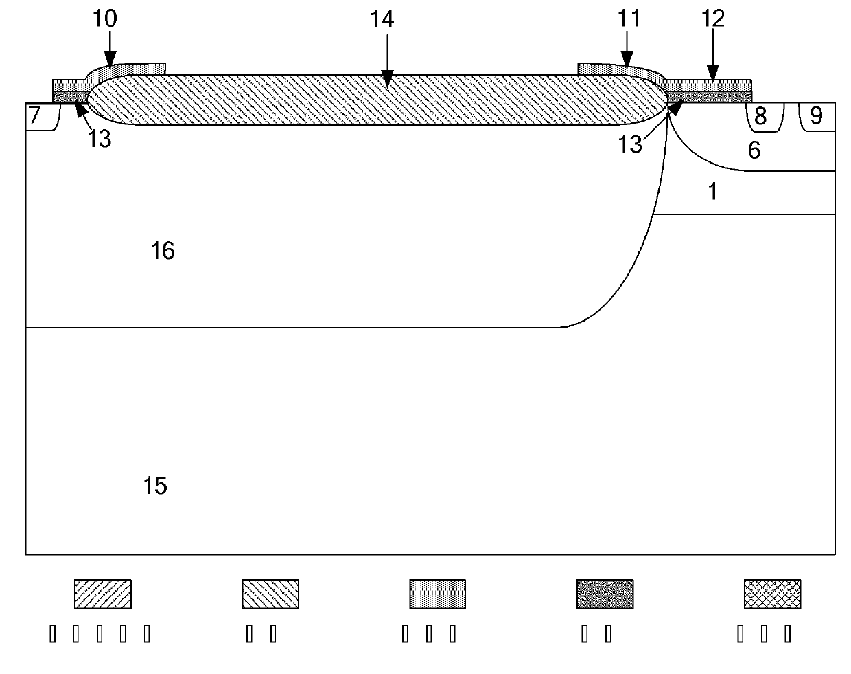
[0055] Embodiment 1: as image 3 As shown, a 700V low on-resistance LDMOS, including P epitaxy 1, P well region 6, N + Anode 7, N + Cathode 8, P + Cathode terminal 9, anode polycrystalline field plate 10, cathode polycrystalline field plate 11, gate polycrystalline 12, gate oxide layer 13, field oxygen layer 14, P substrate 15, N well region 16, P epitaxy 1 and N well The region 16 is located on the P substrate 15, the P well region 6 is located on the P epitaxy 1, and the N + Cathode 8 and P + The cathode terminal 9 is located on the P well region 6, and the N + The anode 7 is positioned on the top of one end of the N well region 16, the field oxide layer 14 is positioned on the N well region 16, and the gate oxide layer 13 at the anode end is positioned on the N well region 16 and is connected with the N well region 16 respectively. + The anode 7 is adjacent to the field oxide layer 14, and the gate oxide layer 13 at the cathode end is located on the P well region 6 an...

Embodiment 2

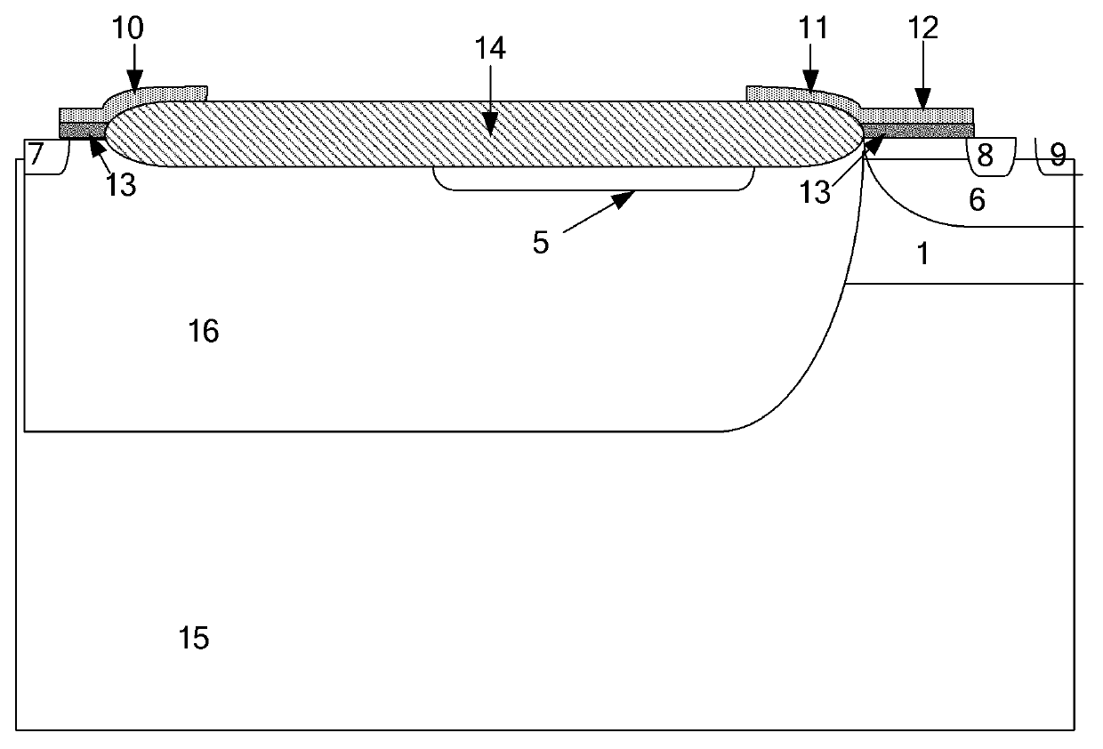
[0079] Embodiment 2: as Figure 4 As shown, the difference between this embodiment and embodiment 1 is that the P buried layer 2 has an N-type conductive channel near the anode, and the rest of the structure is the same as that of embodiment 1, so it will not be repeated here.

[0080] In the forward conduction process of this embodiment, a high potential is applied to the gate polycrystal 12, and an inversion layer is formed on the surface of the cathode end of the gate polycrystal 12, which is located on the surface N of the second N well region 3. + The anode 7 is the drain end of the high voltage LDMOS, and the N in the P well region 6 at the cathode end + The cathode 8 is the source terminal of the structure, and the drain and source terminals are biased with electron flow from N + The cathode 8 is N welled by the inversion layer channel and the second N well region 3 and the first N well region 4 + The anode 7 is collected, and the P-type region 5 is isolated from the ...

Embodiment 3

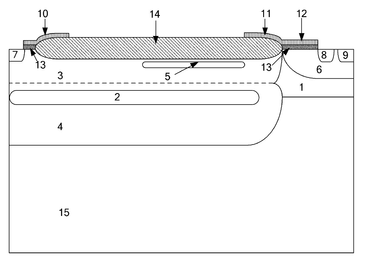
[0085] Embodiment 3: as Figure 5 As shown, the difference between this embodiment and Embodiment 1 is that the P buried layer 2 is a series of isolated islands, the lateral size of each island and the distance between each other are variable, and the P-type region 5 is a series of isolated islands, and each island The lateral dimensions and the distance between them are variable, and the rest of the structure is the same as that of Embodiment 1, so it will not be repeated here.

[0086] In the forward conduction process of this embodiment, a high potential is applied to the gate polycrystal 12, and an inversion layer is formed on the surface of the cathode end of the gate polycrystal 12, which is located on the surface N of the second N well region 3. + The anode 7 is the drain end of the high voltage LDMOS, and the N in the P well region 6 at the cathode end + The cathode 8 is the source terminal of the structure, and the drain and source terminals are biased with electron ...


PUM


Abstract

The invention relates to a high-voltage low-on-resistance lateral double-diffusion metal oxide semiconductor (LDMOS) device and a manufacturing method thereof. The high-voltage low-on-resistance LDMOS device comprises P-epitaxy, a P-well region, an N+ anode, an N+ cathode, a P+ cathode end, an anode multi-crystal field board, a cathode multi-crystal field board, gate polycrystal, a gate oxide, a field oxide layer, a P-substrate, an N-well region and a P-type region, and also comprises the P-type region and a P-buried layer, wherein the P-type region is positioned on the surface of the N-well region; and the P-buried layer is positioned in the N-well region; the P-type region is isolated from the P-well region and the N+ anode, the P-type region is isolated from the field oxide layer; the P-type region and the N-well region form a PN junction; and the N-well region is segmented into a second N-well region and a first N-well region which are positioned above the P-buried layer by using the P-buried layer; and the P-buried layer forms PN junctions with the first N-well region and the second N-well region respectively. The high-voltage low-on-resistance LDMOS device has the advantages that: on one hand, the compatibility of the LDMOS device and a conventional low-voltage Bipolar+metal oxide semiconductor (CMOS)+double-diffusion metal-oxide-semiconductor (DMOS) (BCD) process is improved, on the other hand, the on-resistance of the LDMOS device is reduced on the premise of the same voltage resistance.

Description

technical field [0001] The invention relates to semiconductor high-voltage and low-resistance devices in the field of electronic technology, in particular to high-voltage power devices manufactured on bulk silicon. Background technique [0002] LDMOS devices are high-voltage power devices, which have the characteristics of high operating voltage, relatively simple process, and high switching frequency, and the processing technology based on bulk silicon materials is relatively mature, so LDMOS devices have broad development prospects. The drain, source and gate of the LDMOS device are all located on its surface, which is easy to integrate into the chip, so it is especially suitable as a high-voltage power device in high-voltage integrated circuits (HVIC) and power integrated circuits. Since J.A. Appels proposed the famous RESURF (Reduced Surface Field) principle in 1979, LDMOS devices have developed rapidly. [0003] A conventional LDMOS device in the prior art such as fig...

Claims


Application Information

Patent Timeline
IPC IPC(8): H01L29/78H01L29/06H01L21/336
Inventor 方健吴琼乐陈吕赟王泽华蒋辉管超柏文斌黎莉杨毓俊
Owner UNIV OF ELECTRONIC SCI & TECH OF CHINA
Why Eureka
Try Eureka