Enhanced Raman scattering substrates of silicon semiconductor and a manufacturing method and application for the same
A Raman scattering enhancement, semiconductor technology, applied in Raman scattering, application of thermal effects to detect fluid flow, light guide and other directions, can solve the problems of toxic and side effects of precious metal particles, and achieve the effect of enhancing Raman scattering signals
- Summary
- Abstract
- Description
- Claims
- Application Information
AI Technical Summary
Problems solved by technology
Method used
Image

Examples
Embodiment 1
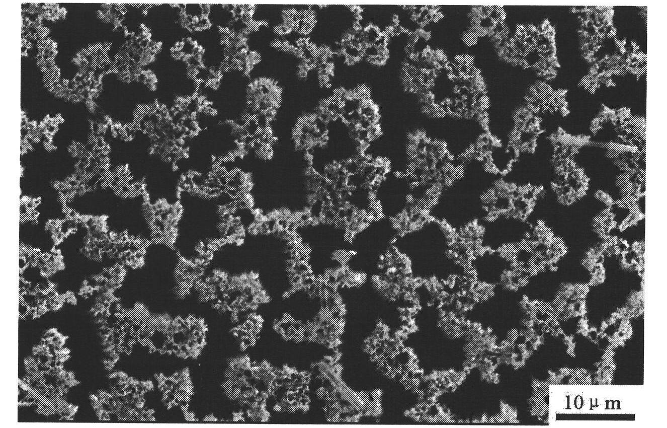
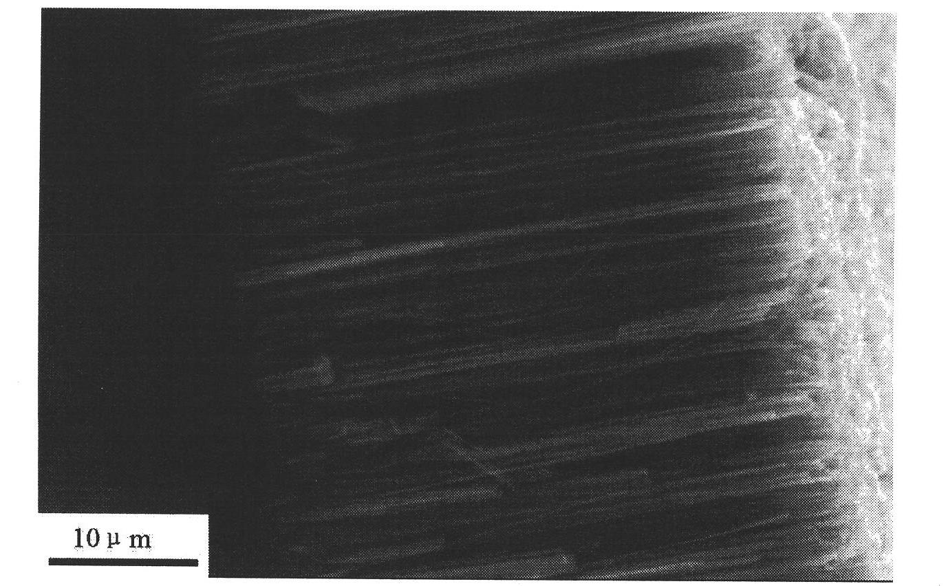
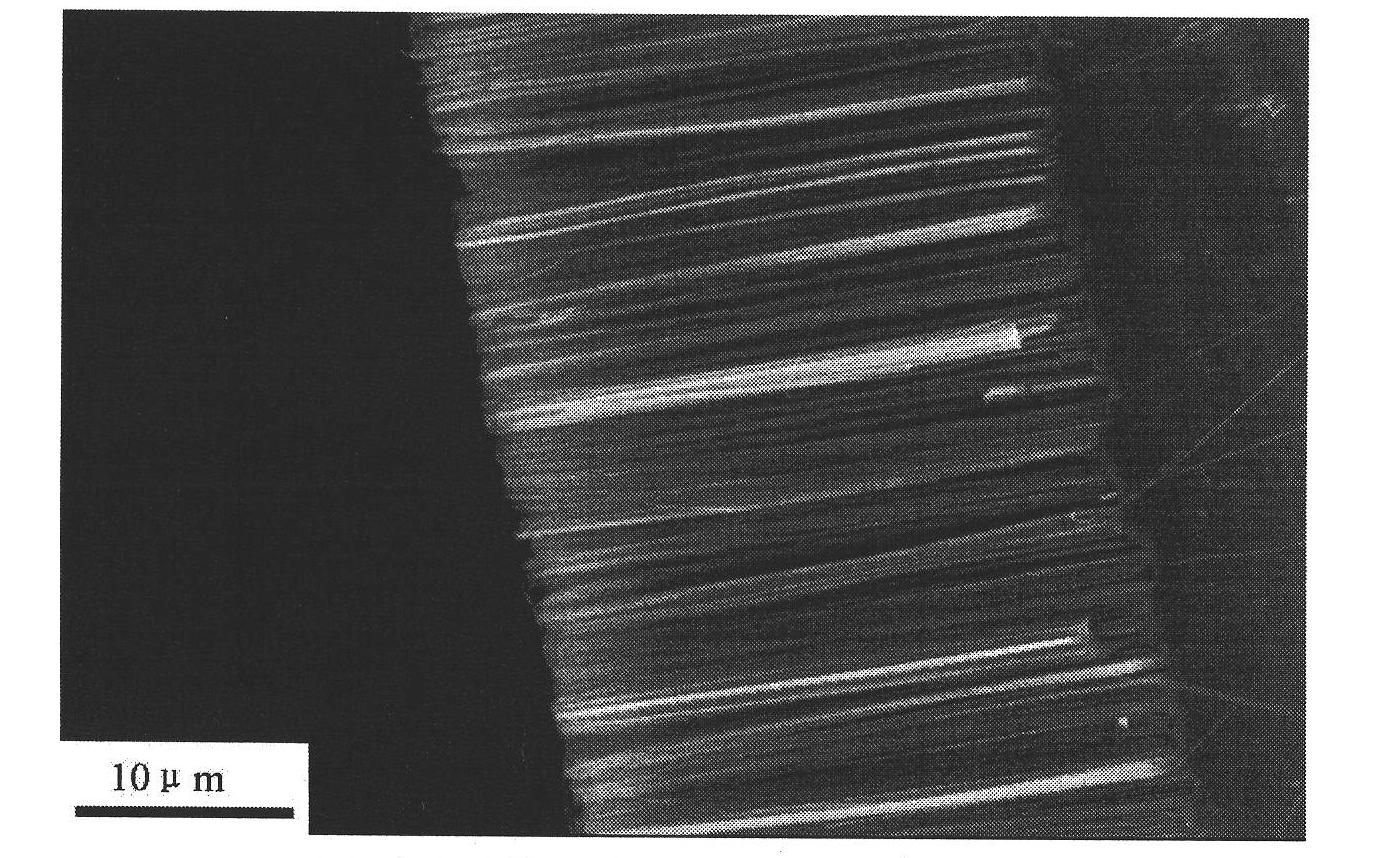
[0038] 1) Soak and clean the P-type (100) monocrystalline silicon substrate in the mixed solution of silver nitrate solution and hydrofluoric acid for 2 minutes and then take it out, wherein the concentration of silver nitrate in the mixed solution is 5 mmol / L, the concentration of hydrofluoric acid is 4.8mol / L; Then the P-type (100) monocrystalline silicon substrate soaked in silver nitrate is placed in a container filled with an etching solution mixed with hydrogen peroxide and hydrofluoric acid for etching Etching for 30 minutes, the container containing the etching solution mixed with hydrogen peroxide and hydrofluoric acid is placed in a water bath, the temperature of the water bath is 50°C, the concentration of hydrogen peroxide in the etching solution is 4mmol / L, and the concentration of hydrofluoric acid is 5.5mol / L; at the place where silver ions are deposited on the surface of the P-type (100) single crystal silicon substrate, Si will be etched down, while at the pla...
Embodiment 2
[0043] 1) Soak and clean the P-type (100) monocrystalline silicon substrate in the mixed solution of silver nitrate solution and hydrofluoric acid for 2.5 minutes and then take it out, wherein the concentration of silver nitrate in the mixed solution is 8 mmol / L, the concentration of hydrofluoric acid is 4.8mol / L; Then the P-type (100) monocrystalline silicon substrate soaked in silver nitrate is placed in a container filled with an etching solution mixed with hydrogen peroxide and hydrofluoric acid for etching Etching for 35 minutes, the container containing the etching solution mixed with hydrogen peroxide and hydrofluoric acid is placed in a water bath, the temperature of the water bath is 40°C, the concentration of hydrogen peroxide in the etching solution is 2mmol / L, and the concentration of hydrofluoric acid is 4.8mol / L; at the place where silver ions are deposited on the surface of the P-type (100) single crystal silicon substrate, Si will be etched down, while at the p...
Embodiment 3
[0047] 1) Soak and clean the P-type (100) monocrystalline silicon substrate in the mixed solution of silver nitrate solution and hydrofluoric acid for 3 minutes and then take it out, wherein the concentration of silver nitrate in the mixed solution is 10mmol / L, the concentration of hydrofluoric acid is 4.8mol / L; Then the P-type (100) monocrystalline silicon substrate soaked in silver nitrate is placed in the container containing the etching solution mixed with hydrogen peroxide and hydrofluoric acid for etching Etching for 25 minutes, the container containing the etching solution mixed with hydrogen peroxide and hydrofluoric acid is placed in a water bath, the temperature of the water bath is 45°C, the concentration of hydrogen peroxide in the etching solution is 3mmol / L, and the concentration of hydrofluoric acid is 5mol / L; at the place where silver ions are deposited on the surface of the P-type (100) single crystal silicon substrate, Si will be etched down, while at the pla...
PUM
| Property | Measurement | Unit |
|---|---|---|
| diameter | aaaaa | aaaaa |
| length | aaaaa | aaaaa |
Abstract
Description
Claims
Application Information
 - R&D
- Intellectual Property
- Life Sciences
- Materials
- Tech Scout
- Unparalleled Data Quality
- Higher Quality Content
- 60% Fewer Hallucinations
Browse by: Latest US Patents, China's latest patents, Technical Efficacy Thesaurus, Application Domain, Technology Topic, Popular Technical Reports.
© 2025 PatSnap. All rights reserved.Legal|Privacy policy|Modern Slavery Act Transparency Statement|Sitemap|About US| Contact US: help@patsnap.com