Thin film transistor liquid crystal display (TFT-LCD) array substrate and manufacturing method thereof

An array substrate and manufacturing method technology, applied in the field of TFT-LCD array substrate and its manufacturing, can solve the problems of unstable performance of thin film transistors, increased defect occurrence rate, large number of masks, etc., achieve fast exposure speed and avoid etching Poor uniformity, effect of reducing process steps

Inactive Publication Date: 2011-04-20
BOE TECH GRP CO LTD +1
View PDF0 Cites 11 Cited by
  • Summary
  • Abstract
  • Description
  • Claims
  • Application Information

AI Technical Summary

Problems solved by technology

[0004] Since each patterning process needs to transfer the pattern of the mask plate to the film pattern, and each layer of film pattern needs to be accurately covered on another layer of film pattern, the five patterning processes in the prior art have complicated processes and production problems. Defects such as long cycle time and a large number of masks used, while a longer process cycle increases the incidence of defects, resulting in a decrease in yield and an increase in cost
However, in the four-step patterning process of the prior art, since the pattern of the TFT channel region is formed by partial exposure and multi-step etching process, the etching uniformity of the pattern of the TFT channel region is poor, and the performance of the thin film transistor is unstable.

Method used


Image

  • Thin film transistor liquid crystal display (TFT-LCD) array substrate and manufacturing method thereof
  • Thin film transistor liquid crystal display (TFT-LCD) array substrate and manufacturing method thereof
  • Thin film transistor liquid crystal display (TFT-LCD) array substrate and manufacturing method thereof

Examples


Embodiment Construction

[0053] The technical solutions of the present invention will be described in further detail below with reference to the accompanying drawings and embodiments.

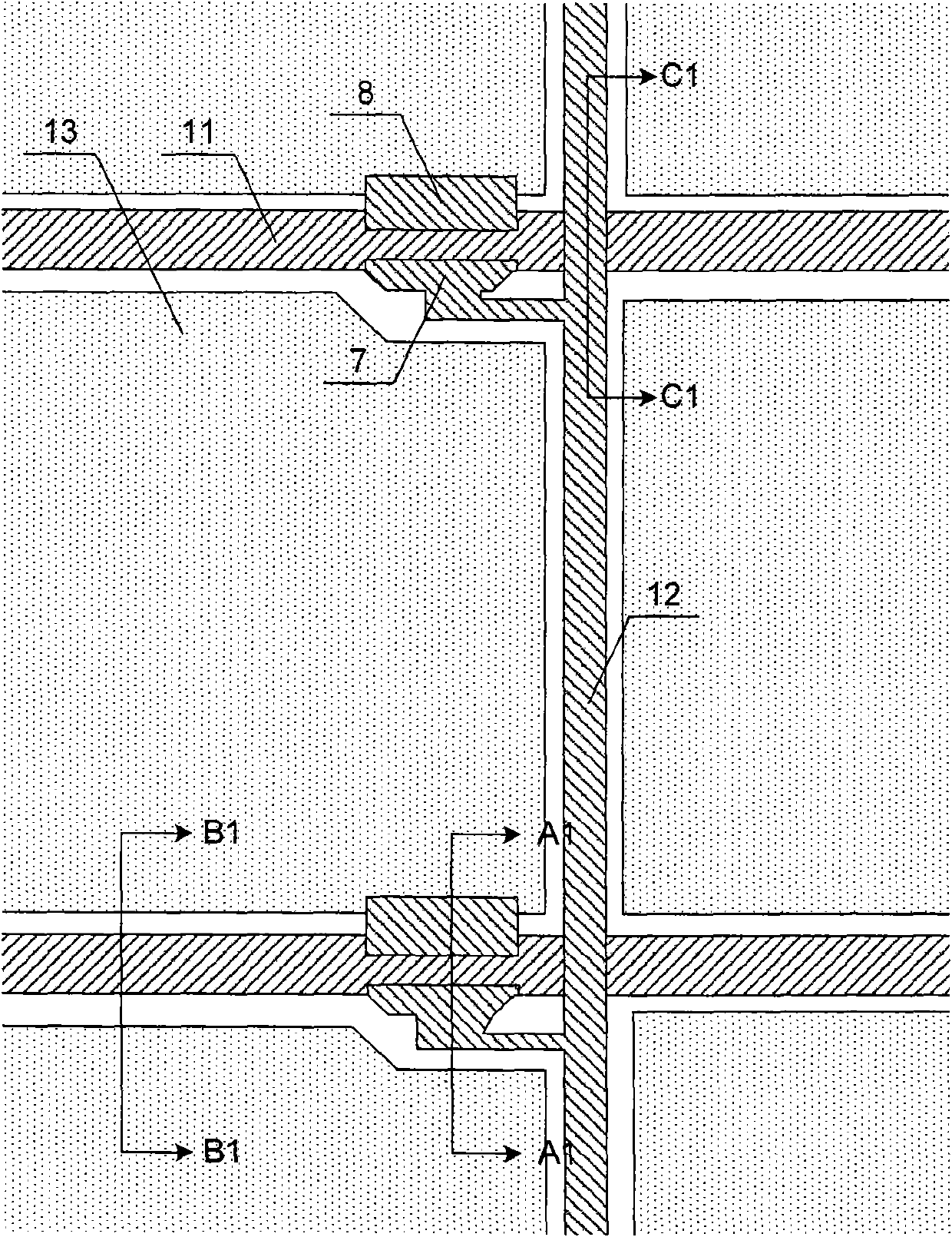
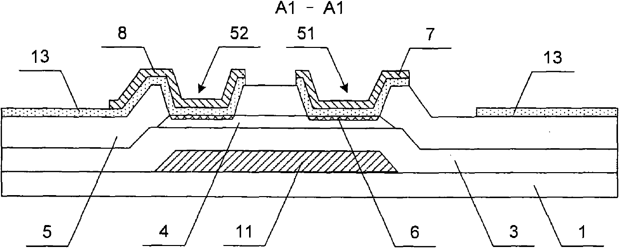
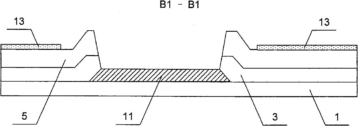
[0054] figure 1 It is a plan view of the first embodiment of the TFT-LCD array substrate of the present invention, reflecting the structure of a pixel unit, figure 2 for figure 1 The cross-sectional view of A1-A1 in the middle, image 3 for figure 1 The sectional view of B1-B1 direction in the middle, Figure 4 for figure 1 The sectional view of C1-C1 direction in the middle, Figure 5 for figure 1 Cross-sectional view of the grid line interface area. Such as Figure 1 to Figure 5 As shown, the main structure of the TFT-LCD array substrate in this embodiment includes gate lines 11, data lines 12, pixel electrodes 13 and thin film transistors, and several gate lines 11 and several data lines 12 perpendicular to each other define several pixel areas A pixel electrode 13 and a thin film transistor are formed in ...


PUM

PropertyMeasurementUnit
thicknessaaaaaaaaaa

Abstract

The invention relates to a thin film transistor liquid crystal display (TFT-LCD) array substrate and a manufacturing method thereof. The manufacturing method comprises the following steps of: depositing a grid metal film, a grid insulation layer and a semiconductor film to form a figure comprising a grid line and a quasi semiconductor layer; depositing a passivation layer to form a semiconductor layer figure, a figure comprising a source electrode via hole and a drain electrode via hole on the semiconductor layer, and a doped semiconductor layer on the surface of the semiconductor layer in the source electrode via hole and the drain electrode via hole; and depositing a transparent conductive film and a source and drain metal film to form a figure comprising a pixel electrode, a data line,a source electrode and a drain electrode, wherein the source electrode is connected with the semiconductor layer through the doped semiconductor layer in the source electrode via hole and the drain electrode is connected with semiconductor layer through the doped semiconductor layer in the drain electrode via hole. The TFT-LCD array substrate can be manufactured through three times of processes, so the process is relatively simple, the process time can be shortened to the maximum extent, the production efficiency is improved, and the production cost is reduced.

Description

technical field [0001] The invention relates to a liquid crystal display and a manufacturing method thereof, in particular to a TFT-LCD array substrate and a manufacturing method thereof. Background technique [0002] At present, the manufacture of thin film transistor liquid crystal display (Thin Film Transistor Liquid Crystal Display, referred to as TFT-LCD) array substrate is completed by forming a pattern through a group of patterning processes. One patterning process forms a layer of patterning. The number of patterning processes can be measured to manufacture TFT- Due to the complexity of the LCD array substrate, reducing the number of patterning processes means reducing the manufacturing cost. The five patterning processes in current technology include: gate line and gate electrode patterning, active layer patterning, source electrode / drain electrode patterning, passivation layer via hole patterning, and pixel electrode patterning. Each patterning process includes thi...

Claims


Application Information

Patent Timeline
Patent Type & Authority Applications(China)
IPC IPC(8): G02F1/1362G02F1/1368H01L27/02H01L21/82
Inventor 谢振宇
Owner BOE TECH GRP CO LTD
Why Eureka
Try Eureka