Integrated power device on silicon on insulator (SOI) layer for negative supply voltage

A technology of negative power supply voltage and integrated power, which is applied in the field of semiconductor power devices, can solve the problems that cannot meet the requirements of the negative power supply voltage working environment, etc., and achieve the effects of low power consumption, reduced process difficulty and cost, and excellent performance

Inactive Publication Date: 2011-04-20
UNIV OF ELECTRONICS SCI & TECH OF CHINA
View PDF5 Cites 13 Cited by
  • Summary
  • Abstract
  • Description
  • Claims
  • Application Information

AI Technical Summary

Problems solved by technology

[0002] Traditional high-voltage integrated circuit devices work in the environment of positive power supply, and have been widely used in motor drive, display drive, automotive ele

Method used


Image

  • Integrated power device on silicon on insulator (SOI) layer for negative supply voltage
  • Integrated power device on silicon on insulator (SOI) layer for negative supply voltage
  • Integrated power device on silicon on insulator (SOI) layer for negative supply voltage

Examples


Embodiment Construction

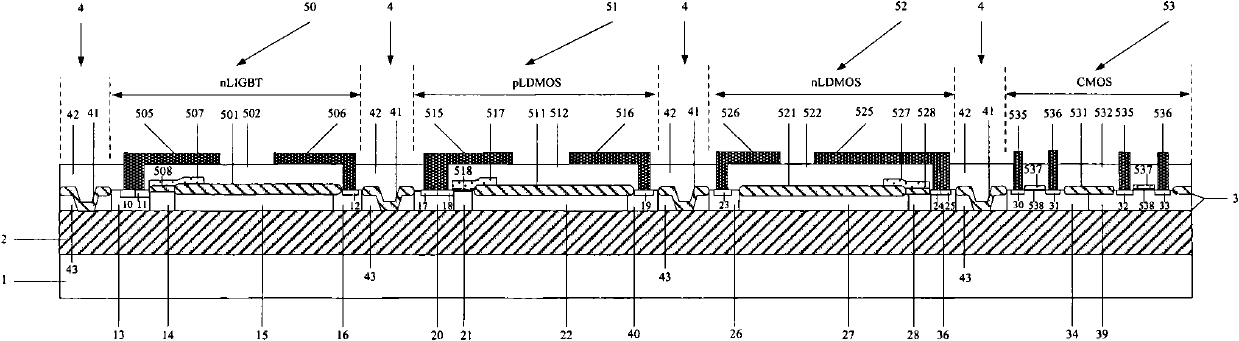
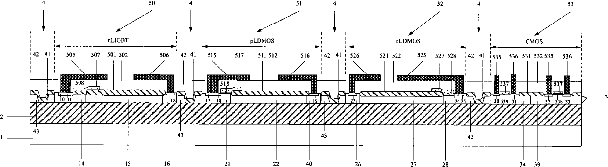
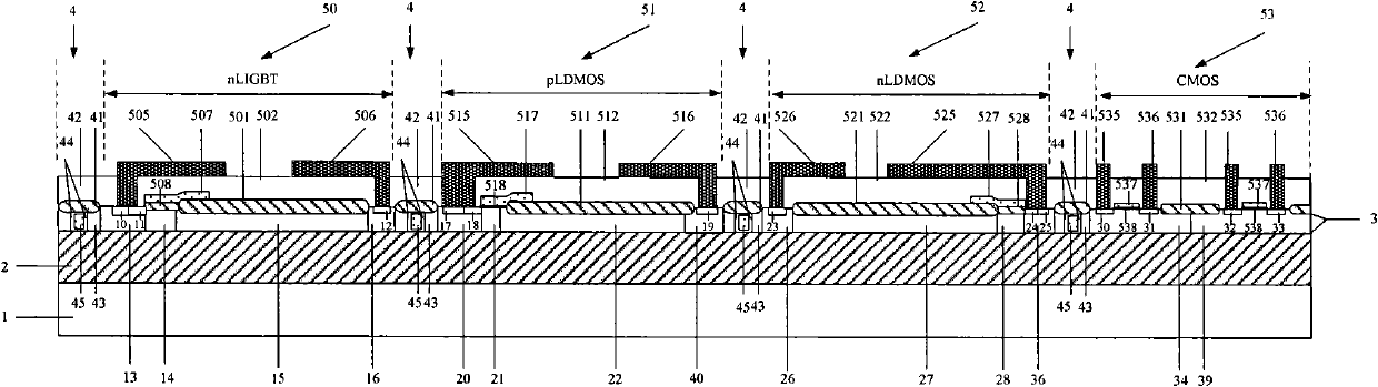
[0022] A thin-layer SOI integrated power device for negative supply voltages, such as Figure 1 to Figure 3 As shown, it includes substrate 1 , buried oxide layer 2 and SOI layer 3 . The buried oxide layer 2 is located between the substrate 1 and the SOI layer 3, and the SOI3 layer is a thin-layer semiconductor with a thickness of 0.5-3 μm. The SOI layer 3 is at least integrated with a high-voltage nLIGBT device (n-channel Lateral Insulated Gate Bipolar Transistors) 50, a high-voltage pLDMOS device (p-channel Lateral Double-diffused MOSFET) 51 and a high-voltage nLDMOS device (n-channel Lateral Double-diffused MOSFET) Two or three devices in MOSFET) 52. Different high-voltage devices are completely isolated by the buried oxide layer 2 and the dielectric isolation region 4 built on the buried oxide layer 2; Slot isolation technology is implemented.

[0023] The SOI layer of the high-voltage nLIGBT device 50 consists of a p-type body region 14, an n-type drift region 15, a p-t...


PUM

PropertyMeasurementUnit
Thicknessaaaaaaaaaa
Electric field strengthaaaaaaaaaa

Abstract

The invention provides an integrated power device on a silicon on insulator (SOI) layer for negative supply voltage, belonging to the field of semiconductor power devices. The integrated power device on the SOI layer for the negative supply voltage is characterized in that the SOI layer is integrated with at least two or three high-voltage devices of an n-type lateral insulated gate bipolar transistor (nLIGBT), a p-type laterally diffused metal oxide semiconductor (pLDMOS) and an n-type laterally diffused metal oxide semiconductor (nLDMOS), and also can be integrated with a low-voltage metal oxide semiconductor (MOS) device; buried oxide layers and dielectrically isolated areas connected with the buried oxide layer are used to realize the complete isolation among the different devices; a conventional local oxidation of silicon (LOCOS) technology or a shallow trench isolation technology is adopted for realizing the dielectrically isolated area; the SOI layer is 0.5-3mu m in thickness; and the dielectric electric-field strength of the thick gate oxide layer of the high-voltage nLIGBT and nLDMOS devices is less than 5*106V/cm so as to meet the requirements of the high-voltage integrated circuit of the negative supply voltage for high voltage resistance between the grid electrodes and source electrodes of the devices. The integrated power device on a SOI layer for the negative supply voltage has the advantages of small parasitic effect, fast speed, low power consumption, strong irradiation resistance and the like, realizes compatibility of the high-voltage devices with the low-voltage devices, and meets the requirements of the working environment of the negative supply voltage. The integrated power device on a SOI layer for the negative supply voltage is used to manufacture a plurality of high-voltage, high-speed and low conducting-loss power devices with good performances, and is used for the high-voltage application of the negative supply voltage.

Description

technical field [0001] The invention belongs to the technical field of semiconductor power devices, relates to an integrated semiconductor device, in particular to a negative power supply voltage thin-layer SOI integrated semiconductor device applied to a high-voltage power integrated circuit. Background technique [0002] Traditional high-voltage integrated circuit devices work in the environment of positive power supply, and have been widely used in motor drive, display drive, automotive electronics and other fields, but the structure of traditional high-voltage integrated circuit device cannot meet the working environment requirements of negative power supply voltage. Contents of the invention [0003] The invention provides a negative power supply voltage thin-layer SOI integrated semiconductor device applied to high-voltage power integrated circuits. This high-voltage integrated semiconductor device fully utilizes the advantages of low leakage and low power consumption...

Claims


Application Information

Patent Timeline
IPC IPC(8): H01L27/12
Inventor 乔明王猛胡曦庄翔赖力赵远远张波
Owner UNIV OF ELECTRONICS SCI & TECH OF CHINA
Why Eureka
Try Eureka