

Metal surface plated nickel/gold treatment method of ceramic metalized substrate and manufactured ceramic metalized substrate
A technology of ceramic metallization and nickel-gold electroplating, which is applied in the field of semiconductor manufacturing and ceramic metallization substrates, can solve the problems of decreased reliability of solder joints, very high requirements for solderability and solder joint reliability, and protruding edges of the coating layer. Solve the protruding edge of the coating, suitable for large-scale popularization and application, and the effect of unique and ingenious design
- Summary
- Abstract
- Description
- Claims
- Application Information
AI Technical Summary
Problems solved by technology
Method used
Image

Examples
Embodiment Construction
[0034] In order to understand the technical content of the present invention more clearly, the following examples are given in detail. The ceramic metallized substrate takes a copper-clad ceramic substrate (DBC) substrate as an example, and the deposited metal is copper.
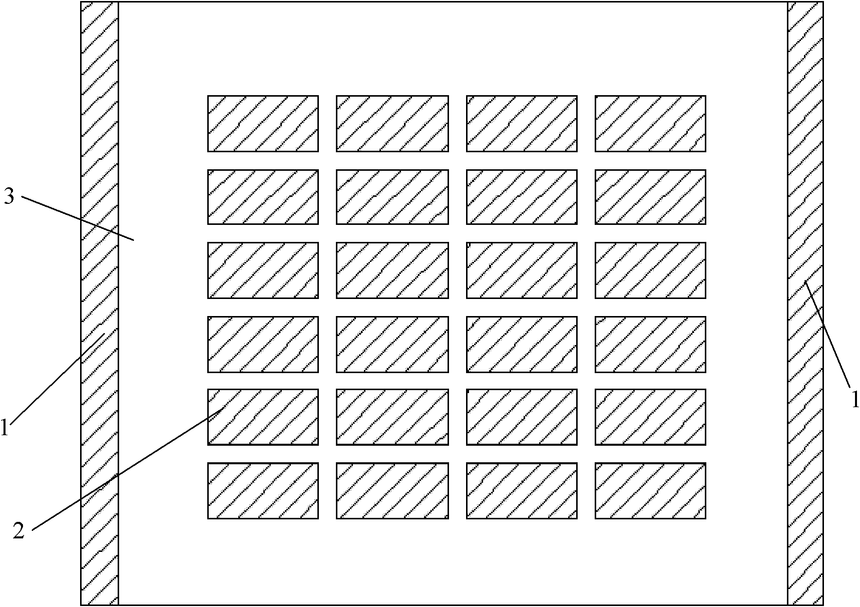
[0035] ●Making DBC substrates with conductive edges
[0036] Negative production process:
[0037] Raw materials (copper sheets, ceramics)-cleaning-sintering-pretreatment-attaching dry resist film-exposure and development-acid etching-removal of film.
[0038] Process conditions
[0039] Concentration of pretreatment microetching solution: sulfuric acid 90-200g / l; sodium persulfate 80-150g / l;
[0040] Temperature: 30℃±10℃
[0041] Time: 60s~120s
[0042] The finished DBC substrate with conductive edges is shown in figure 1 .
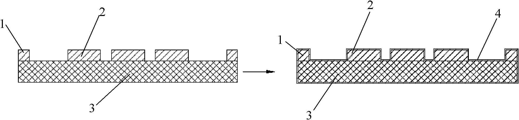
[0043] ●Ceramic sinking copper
[0044] Ceramic copper deposition technology (that is, the aforementioned ceramic deposition metal technolog...
PUM
| Property | Measurement | Unit |
|---|---|---|
| Thickness | aaaaa | aaaaa |
| Thickness | aaaaa | aaaaa |
| Thickness | aaaaa | aaaaa |
Abstract
Description
Claims
Application Information