Gallium nitride (GaN) enhancement type metal insulator semiconductor field effect transistor (MISFET) device and manufacturing method thereof

An enhanced, device technology, used in semiconductor/solid-state device manufacturing, semiconductor devices, electrical components, etc., can solve the problems of increasing device on-resistance, low current density, affecting device performance, etc., to increase device current density. , the effect of reducing gate leakage current and increasing threshold voltage

Inactive Publication Date: 2011-06-01
SUN YAT SEN UNIV
View PDF5 Cites 14 Cited by
  • Summary
  • Abstract
  • Description
  • Claims
  • Application Information

AI Technical Summary

Problems solved by technology

However, the current GaN-based MISFET based on the traditional MISFET structure has a small conduction current, which is not conducive to the realization of high-power characteristics; The etching process, and the damage caused by the etching process to the material affects the performance of the device. After etching, the alignment of the conductive channel plane under the gate and the source-drain conductive channel plane cannot be accurately controlled, which increases the on-resistance of the device and the current density. Low

Method used


Image

  • Gallium nitride (GaN) enhancement type metal insulator semiconductor field effect transistor (MISFET) device and manufacturing method thereof
  • Gallium nitride (GaN) enhancement type metal insulator semiconductor field effect transistor (MISFET) device and manufacturing method thereof
  • Gallium nitride (GaN) enhancement type metal insulator semiconductor field effect transistor (MISFET) device and manufacturing method thereof

Examples


Embodiment 1

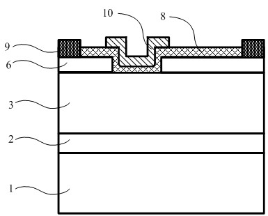
[0034] This example figure 1 A GaN enhanced MISFET device is given, which includes: a substrate 1, a stress buffer layer 2 and a GaN layer 3 grown on the substrate 1 by MOCVD or MBE, and a heterogeneous layer 6 selectively grown on the GaN layer 3 During selective growth, a heterogeneous layer structure is grown in the access region, and the gate is blocked by the mask layer 5, the gate region is deposited to form an insulating dielectric layer 8, and the source and drain access regions are vapor-deposited with ohmic contact metal 9, A gate metal 10 is vapor-deposited on the insulating dielectric layer in the gate region.

[0035] The thickness of the growing heterogeneous layer 6 needs to be controlled to not only form a sufficient two-dimensional electron gas concentration at the interface of the GaN layer, but also reduce the ohmic contact resistance of the source and drain and the on-resistance of the device. The thickness of the heterogeneous layer can be controlled with...

Embodiment 2

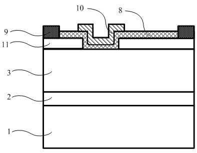
[0038] Such as figure 2 As shown, this embodiment provides a second structure of a GaN enhanced MISFET device, which is roughly the same as the device structure of Embodiment 1, the difference is that when the heterogeneous layer 11 is selectively grown, the N-type doped It further reduces the ohmic contact resistance of the source and drain regions and increases the current density of the device.

Embodiment 3

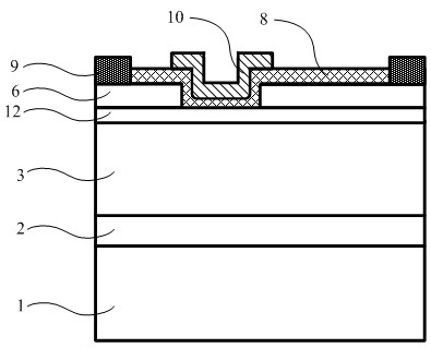
[0040] Such as image 3 As shown, this embodiment provides a third structure of a GaN enhanced MISFET device. In this embodiment, a 1nm-10nm AlN insertion layer 12 is grown on the surface of the GaN layer 3 in the conductive channel region, and the AlN The insertion layer 12 can effectively increase the concentration and mobility of the conductive channel 2DEG, and increase the on-current density of the device. The specific solution is that after the GaN layer 3 is grown on the substrate material, the AlN insertion layer 12 is grown, and the subsequent process is the same as that of the embodiment 1.


PUM


Abstract

The invention relates to a gallium nitride (GaN) enhancement type metal insulator semiconductor field effect transistor (MISFET) device and a manufacturing method thereof. The GaN enhancement type MISFET device comprises a substrate and an epitaxial layer arranged on the substrate, wherein the epitaxial layer comprises a stress buffer layer and a GaN layer sequentially from bottom to top; a heterogeneous layer selectively grows on the GaN layer; insulating medium layers are formed on the surface, where the heterogeneous layer does not grow, of the GaN layer and the surface of the heterogeneous layer; a grid region is arranged on the insulating medium layer formed on the surface of the GaN layer; the insulating medium layer formed on the surface of the heterogeneous layer is etched to form a source region and a drain region; grid metals are formed in the grid region; and ohmic contact metals are formed on the source region and the drain region. The GaN enhancement type MISFET device and the manufacturing method thereof have the characteristics that: a heterogeneous structure with high-concentration two-dimensional electron gas grows in an access region by a selected region epitaxial technique, so that the conducting channel plane of the grid can naturally align with that of the source and the drain, the resistance of the access region can be effectively reduced, and the threshold voltage of the grid of the device can be increased.

Description

technical field [0001] The invention relates to a GaN enhanced MISFET device and a preparation method thereof, in particular to a GaN enhanced MISFET device used in high temperature and high power switching devices and microwave devices and a preparation method thereof. Background technique [0002] The wide bandgap semiconductor material represented by GaN has excellent material properties such as wide bandgap, high breakdown electric field strength, high thermal conductivity, high saturation electron drift velocity, and high concentration of two-dimensional electron gas at the heterogeneous interface; it has become the third research hotspots in semiconductors. These characteristics make GaN have great advantages and application prospects in the manufacture of high-power electronic devices. [0003] The study of enhanced (normally off) HEMT is of great significance to the practical application of GaN electronic devices. The gate of the enhanced device can close the chann...

Claims


Application Information

Patent Timeline
Patent Type & Authority Applications(China)
IPC IPC(8): H01L29/78H01L29/06H01L21/336
Inventor 刘扬贺致远姚尧
Owner SUN YAT SEN UNIV
Why Eureka
Try Eureka