

Method for preparing periodic nanostructure with high aspect ratio
A nanostructure, high aspect ratio technology, applied in the field of high aspect ratio periodic nanostructures using interference lithography and three-layer glue technology, can solve the problem that photoresist cannot provide enough anti-etching layer, and achieve low cost , Wide application prospect, high efficiency effect
Inactive Publication Date: 2011-06-15
INST OF OPTICS & ELECTRONICS - CHINESE ACAD OF SCI
View PDF7 Cites 18 Cited by
- Summary
- Abstract
- Description
- Claims
- Application Information
AI Technical Summary
Problems solved by technology
Method used
View moreImage
Smart ImageViewing Examples

Examples
Embodiment 1
Embodiment 2
Embodiment 3
Login to View More PUM
| Property | Measurement | Unit |
|---|---|---|
| Thickness | aaaaa | aaaaa |
| Thickness | aaaaa | aaaaa |
| Thickness | aaaaa | aaaaa |
Abstract
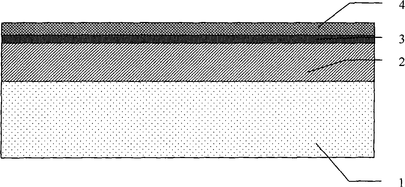
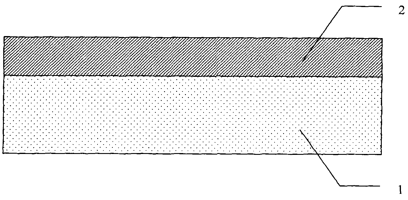
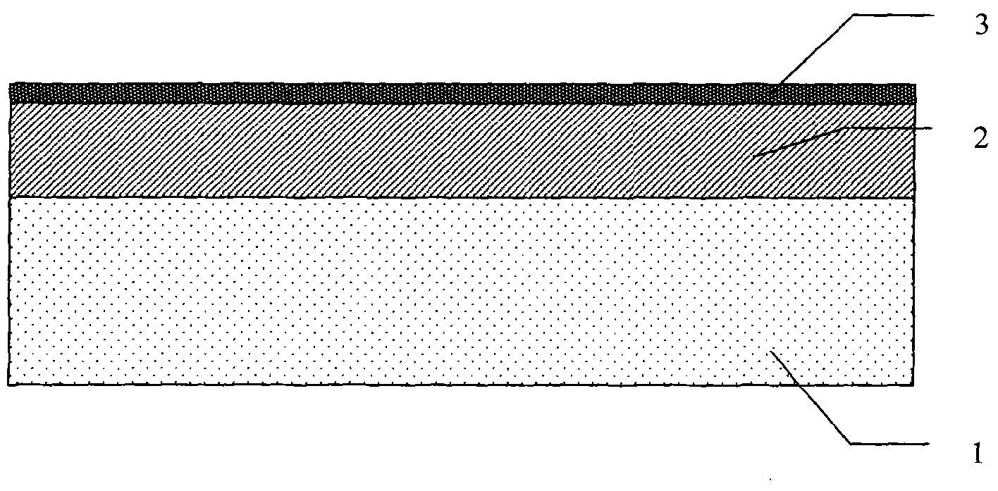
The invention discloses a method for preparing a periodic nanostructure with high aspect ratio. The method is characterized by comprising the following steps of: selecting a polished substrate; coating a layer of photoresist with the thickness of greater than or equal to 300 nm on the surface of the polished substrate by a spin-coating method; depositing a SiO2 film with the thickness of 20 nm on the surface of the photoresist by a magnetron sputtering method; coating a layer of high-resolution photoresist with the thickness of 50 to 100 nm on the surface of the SiO2 film by the spin-coating method; exposing and developing the surface high-resolution photoresist by utilizing laser interference photolithography; hardening the three-layer adhesive structure in a heating plate or a baking oven; selecting a fluorine-base gas; transferring a surface photoresist pattern to the SiO2 layer by utilizing reactive ion etching; selecting and using oxygen; taking the SiO2 layer as a hard mask layer; and transferring a pattern on the SiO2 layer to the bottom photoresist by utilizing the reactive ion etching to obtain a photoresist pattern with high resolution and high aspect ratio. The method has low cost, large area of processed pattern area, and a broad application prospect in the aspects of the manufacturing and the application research of sub-wavelength gratings and photonic crystals.
Description
A method for fabricating high aspect ratio periodic nanostructures technical field The invention relates to a method for manufacturing a high-aspect-ratio periodic nanostructure, in particular to a method for manufacturing a high-aspect-ratio periodic nanostructure by using interference photolithography and three-layer adhesive technology. technical background Subwavelength periodic nanostructures have attracted extensive attention due to their special optical properties and physical effects. For example, photonic crystals based on semiconductor energy band theory can manipulate light waves by introducing defects, making it possible to realize "integrated optical circuits"; artificial materials based on surface plasmon polaritons (SPPs) effects can modulate light The amplitude and phase distribution of the field realize the negative refraction of light, which has broad application prospects in super-resolution imaging, SPPs nanolithography and other fields. Both photonic...
Claims
Login to View More Application Information
Patent Timeline
 IPC IPC(8): G03F7/00G03F7/09B82Y40/00
Inventor方亮罗先刚王长涛刘玲冯沁赖之安杨欢
OwnerINST OF OPTICS & ELECTRONICS - CHINESE ACAD OF SCI