Anti-charged dust device used on surface of optical system or solar cell

A technology of solar cells and optical systems, applied in photovoltaic power generation, circuits, electrical components, etc., can solve the problems of optical system image quality impact, limit the application of dust removal electric curtains, etc., achieve good dust prevention and dust removal effects, good hydrophobicity and natural Cleaning function, effect of increased roughness

Active Publication Date: 2011-06-29
ZHEJIANG UNIV
View PDF5 Cites 12 Cited by
  • Summary
  • Abstract
  • Description
  • Claims
  • Application Information

AI Technical Summary

Problems solved by technology

However, because the dust removal electric curtain may affect the imaging quality of the optical system, and the parameters such as electrode width, electrode spacing and AC v

Method used


Image

  • Anti-charged dust device used on surface of optical system or solar cell
  • Anti-charged dust device used on surface of optical system or solar cell
  • Anti-charged dust device used on surface of optical system or solar cell

Examples


Example Embodiment

[0024] Example 1

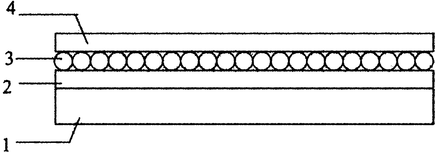
[0025] Such as figure 1 As shown, a device for preventing charged dust on the surface of a solar cell is composed of a substrate 1, and an indium tin oxide layer 2, a titanium dioxide nanoparticle array layer 3, and a fluoropolymer film layer sequentially formed on the substrate 1. 4 constitute.

[0026] Among them, the substrate 1 is a p-type single crystal silicon wafer used on the surface of the solar cell; the indium tin oxide layer 2 is a transparent indium tin oxide layer; the titanium dioxide particle size in the titanium dioxide nanoparticle array layer 3 is 5 microns, The achievable roughness of the titanium dioxide nanoparticle array layer is 2; the fluoropolymer film layer 4 is a polytetrafluoroethylene layer with a thickness of 5 microns.
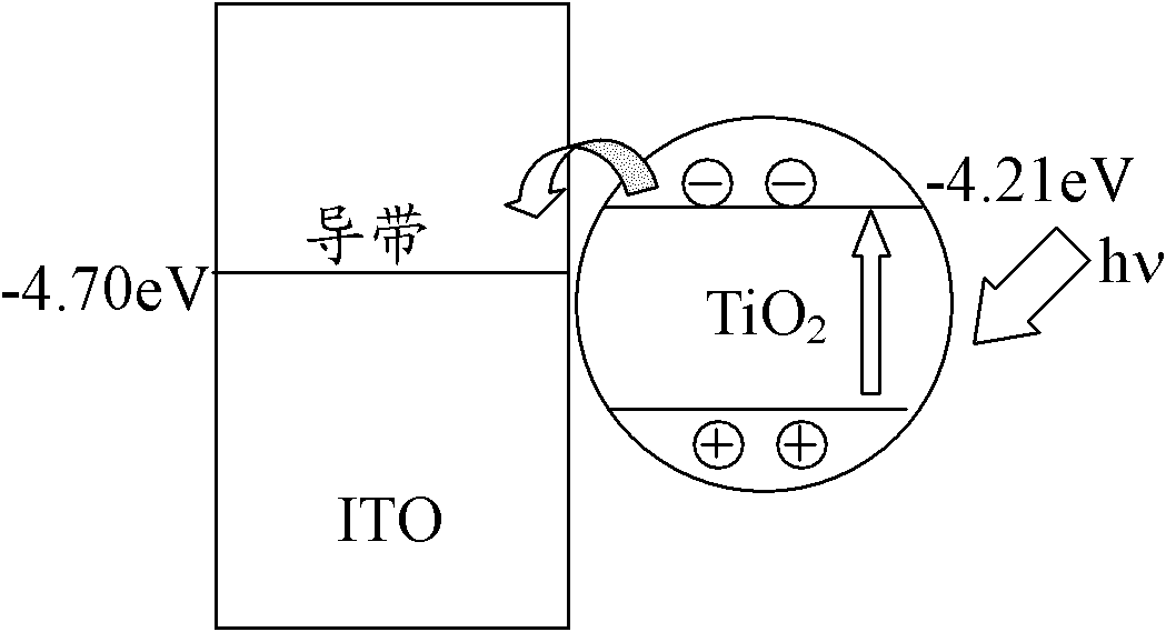
[0027] Such as figure 2 As shown, under ultraviolet light, the conduction band energy level of titanium dioxide in the titanium dioxide nanoparticle array layer 3 is -4.21 eV, and the conduction band energy level ...

Example Embodiment

[0028] Example 2

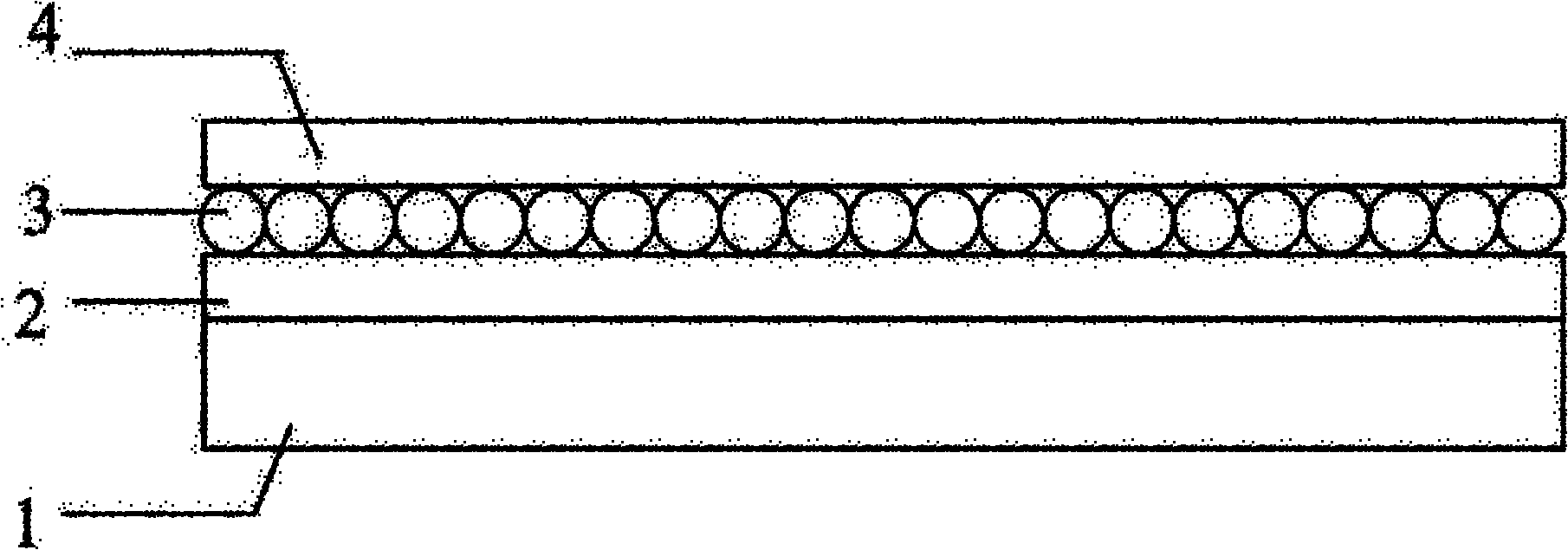
[0029] A device for preventing charged dust on the surface of an optical system is composed of a substrate 1, and an indium tin oxide layer 2, a titanium dioxide nanoparticle array layer 3, and a fluoropolymer film layer 4 sequentially formed on the substrate 1.

[0030] Among them, the substrate 1 is K9 glass used on the surface of the optical system; the indium tin oxide layer 2 is a transparent indium tin oxide layer; the particle size of the titanium dioxide in the titanium dioxide nanoparticle array layer 3 is 50 nm, and the size of the titanium dioxide particle array layer is The roughness is 2; the fluoropolymer film layer 4 is a polyvinylidene fluoride layer with a thickness of less than 100 nm.

[0031] The mechanism is the same as that in Example 1, but the tolerance temperature range of polyvinylidene fluoride and polytetrafluoroethylene in the fluoropolymer layer is different. The tolerance temperature of polytetrafluoroethylene is -196~260℃. The toler...


PUM

PropertyMeasurementUnit
Particle sizeaaaaaaaaaa
Thicknessaaaaaaaaaa
Particle sizeaaaaaaaaaa

Abstract

The invention discloses an anti-charged dust device used on the surface of an optical system or a solar cell, comprising a substrate, as well as a tin indium oxide layer, a titanium dioxide nanoparticle array layer and a fluorine-containing polymer thin film layer, which are sequentially formed on the substrate, and the substrate is glass used on the surface of the optical system or a silicon chip used on the surface of the solar cell. Under continuous ultraviolet radiation, the surface of the device is continuously positively charged, thereby enabling dust adhered on the surface to finally have the same charge with that on the surface of the device regardless of the original charge of the dust, and further enabling dust particles to be separated from the surface under the action of electrostatic repulsion. In addition, a hole generated by the titanium dioxide layer under the ultraviolet radiation has strong oxidizing property, thereby being capable of decomposing organic matters adhered on the surface of an optical device and playing a bactericidal role. The device can achieve good dust prevention and dust removal effects, and effectively prevent light transmittance on the surface of the optical system or the solar cell from being reduced due to hindrance of the dust.

Description

technical field [0001] The invention belongs to the field of dust protection devices, and in particular relates to a device for preventing charged dust on the surface of an optical system or a solar cell. Background technique [0002] With the rapid development of science and technology, optical systems have been widely used. For optical systems, the hazards of dust cannot be ignored. Dust particles will be charged under the action of the external environment, and under the action of electrostatic force, stick and accumulate on various devices that come into contact with the optical system, resulting in blurred vision, seal failure, reading errors, material wear, mechanism blockage, There are many problems such as a significant decrease in image contrast, a significant reduction in luminous flux, and dust contamination of the camera filter. Therefore, it is necessary to protect the optical system from dust, that is, to take dust prevention and dust removal measures for its...

Claims


Application Information

Patent Timeline
IPC IPC(8): H01L31/04H01L31/0216
CPCY02E10/50
Inventor 马海敏尹伊许坚叶辉刘旭
Owner ZHEJIANG UNIV
Why Eureka
Try Eureka