Preparation method of germanium-based Schottky N-type field effect transistor

A field effect transistor, MOS transistor technology, applied in the field of VLSI process manufacturing

Active Publication Date: 2011-07-27
SEMICONDUCTOR MANUFACTURING INTERNATIONAL (BEIJING) CORP +1
View PDF5 Cites 15 Cited by
  • Summary
  • Abstract
  • Description
  • Claims
  • Application Information

AI Technical Summary

Problems solved by technology

In addition, the gate dielectric of germanium-based MOS devices also has major problems. Generally, an interfacial layer needs to be inserted to improve gate capacitance performance.

Method used


Image

  • Preparation method of germanium-based Schottky N-type field effect transistor
  • Preparation method of germanium-based Schottky N-type field effect transistor
  • Preparation method of germanium-based Schottky N-type field effect transistor

Examples


Embodiment Construction

[0026] Below in conjunction with accompanying drawing and specific embodiment the present invention is described in further detail:

[0027] With reference to Fig. 1, the present invention provides a preferred embodiment to illustrate the preparation method of germanium-based Schottky NMOS transistor of the present invention, and this method comprises the steps:

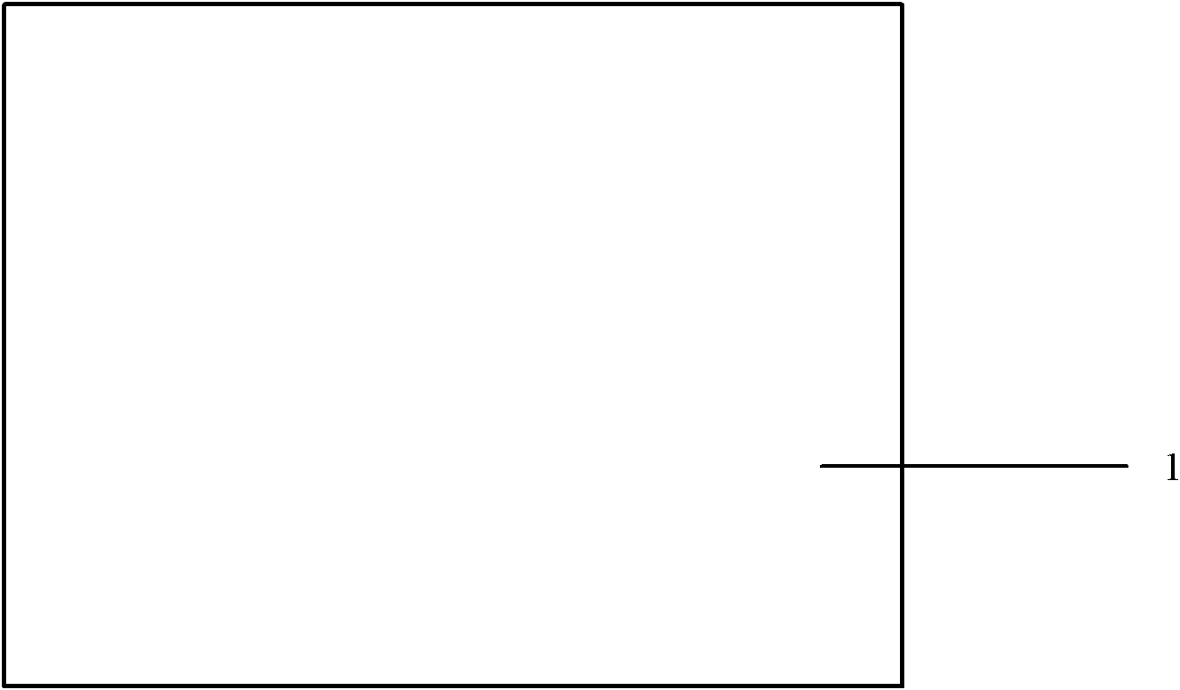
[0028] Step 1: Provide a germanium-based substrate. As shown in FIG. 1(a), a P-type semiconductor germanium substrate 1, wherein the semiconductor germanium substrate 1 can be a bulk germanium substrate, a germanium-on-insulator (GOI) substrate, or an epitaxial germanium substrate.

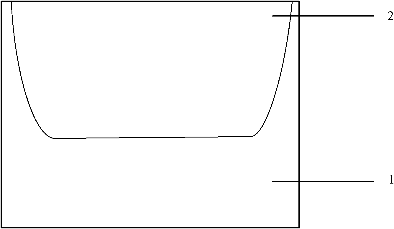
[0029] Step 2: Fabricate the N-well region. Deposit a silicon oxide layer and a silicon nitride layer on the germanium substrate, define the N well region by photolithography, reactive ion etch away the silicon nitride in the N well region, and ion implant N-type impurities, such as phosphorus, and then Annealing is driven in to make N...


PUM

PropertyMeasurementUnit
thicknessaaaaaaaaaa
thicknessaaaaaaaaaa

Abstract

The invention provides a preparation method of a germanium-based Schottky N-type field effect transistor, belonging to the technical field of technical manufacturing of ultra large scale integrations (ULSI). In the preparation method, a high-k medium thin layer is formed among a germanium substrate, a metal source and a metal drain. On one hand, the thin layer can prevent an electron wave function in metal from introducing an MIGS (Metal Induction Gap Strip) interface state into a semiconductor forbidden band and can passivate a dangling bond of a germanium interface; and on the other hand, an insulating medium layer is very thin and electrons can freely pass through the insulating medium layer basically, so that the parasitic resistances of the source and the drain cannot be increased remarkably. By adopting the method, the Fermi level pinning effect can be wakened, the Fermi level is close to the conduction band position of germanium, and the electronic barrier is lowered, therefore, the electric current on-off ratio of the germanium-based Schottky transistor is increased, and the performance of an NMOS (Negative Channel Metal Oxide Semiconductor) device is improved.

Description

technical field [0001] The invention belongs to the technical field of ultra-large-scale integrated circuit (ULSI) manufacturing technology, and in particular relates to a preparation method of a germanium-based Schottky N-type field-effect (NMOS) transistor. Background technique [0002] With the continuous shrinking of the feature size of CMOS devices, the development of traditional silicon-based MOS devices has gradually reached the dual limits of physics and technology, and the degradation of carrier mobility has become a key factor affecting the further improvement of device performance. In order to improve the driving ability of the device, the use of high-mobility channel materials is a very effective way. The hole mobility of germanium material under low electric field is 4 times that of silicon material, and the electron mobility is 2 times that of silicon material. Therefore, as a new channel material, germanium material has a higher and more symmetrical current ca...

Claims


Application Information

Patent Timeline
Patent Type & Authority Applications(China)
IPC IPC(8): H01L21/336H01L29/47H01L29/78
CPCH01L29/41783H01L29/66643H01L29/0895H01L29/78H01L29/517
Inventor 李志强郭岳安霞云全新黄英龙黄如张兴
Owner SEMICONDUCTOR MANUFACTURING INTERNATIONAL (BEIJING) CORP
Why Eureka
Try Eureka