Photosensitive resin composition, photosensitive resin laminate, method for forming resist pattern, conductive pattern, and method for manufacturing printed wiring board

A photosensitive resin layer and photosensitive resin technology, which is applied in the manufacture of printed circuits, printed circuits, removal of conductive materials by chemical/electrolytic methods, etc. Excellent focus and excellent masking effect

Active Publication Date: 2015-06-10
ASAHI KASEI KK
View PDF4 Cites 8 Cited by
  • Summary
  • Abstract
  • Description
  • Claims
  • Application Information

AI Technical Summary

Problems solved by technology

In addition, in the masking method and the plating method, the adhesion between the resist and copper is important in order not to infiltrate the etching solution and the plating solution between the resist and copper, but as the adhesion increases, there is The problem that the peeling time will become longer
[0006] Patent Document 1 describes a photosensitive resin composition containing a chain copolymer of ethylene oxide and propylene oxide in order to improve masking properties while maintaining the high resolution and high adhesion of the photosensitive resin composition, But there is no record of the problem of detachability

Method used


Image

  • Photosensitive resin composition, photosensitive resin laminate, method for forming resist pattern, conductive pattern, and method for manufacturing printed wiring board
  • Photosensitive resin composition, photosensitive resin laminate, method for forming resist pattern, conductive pattern, and method for manufacturing printed wiring board
  • Photosensitive resin composition, photosensitive resin laminate, method for forming resist pattern, conductive pattern, and method for manufacturing printed wiring board

Examples


Embodiment 1~13、 comparative example 1 and 2

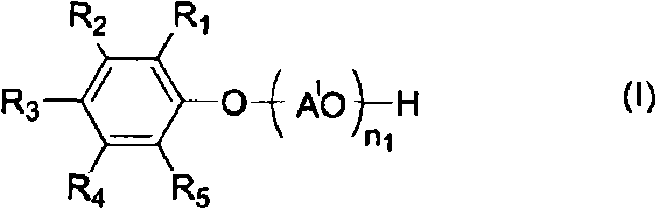
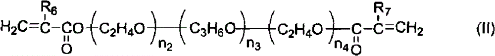
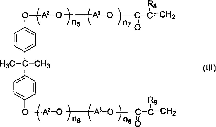
[0137] The compounds shown in Table 1 were mixed in parts by mass shown in Table 2 and Table 3 to obtain a photosensitive resin composition. In addition, in Table 2 and Table 3, MEK represents methyl ethyl ketone, and the mass parts in the composition ratio of the compound other than MEK refer to the value calculated including MEK in the total amount.

[0138] 1. Preparation of samples for evaluation

[0139] The photosensitive resin laminates in Examples and Comparative Examples were produced as follows.

[0140]

[0141] Fully stir and mix the photosensitive resin composition of each embodiment and each comparative example, and use a bar coater to uniformly coat each composition on a 16 μm thick polyethylene terephthalate as a support. The surface of the film was dried in a dryer at 95° C. for 4 minutes to form a photosensitive resin layer. The thickness of the photosensitive resin layer was 40 μm.

[0142] Next, on the surface of the photosensitive resin layer on which...


PUM

PropertyMeasurementUnit
thicknessaaaaaaaaaa
particle diameteraaaaaaaaaa
thicknessaaaaaaaaaa

Abstract

A photosensitive resin composition providing excellent resolution, adhesion, tinting properties and releasability.  The photosensitive resin composition contains (a) a thermoplastic polymer obtained by polymerizing, as a polymerization component, at least a,ß-unsaturated carboxyl group-containing monomer, and having an acid equivalent weight of 100-600 and a weight average molecular weight of 5,000-500,000, (b) an addition-polymerizable monomer having at least one polymerizable ethylenically unsaturated bond in each molecule, (c) a photopolymerization initiator and (d) a compound represented by general formula (I). (In the formula, R1-R5 independently represent an H, an aryl group or an arylalkyl group, and at least one of R1-R5 represents an aryl group or an arylalkyl group; A1 represents C2H4 or C3H6, and when n1 is not less than 2, the plurality of A1's may be the same as or different from each other; and n1 represents an integer of 1-50.)

Description

technical field [0001] The present invention relates to a photosensitive resin composition that can be developed by an alkaline aqueous solution, a photosensitive resin laminate obtained by laminating the photosensitive resin composition on a support, and a substrate using the photosensitive resin laminate A method of forming a resist pattern and uses of the resist pattern. More specifically, it relates to a photosensitive resin composition capable of providing a resist pattern suitable for use in the manufacture of printed circuit boards, the manufacture of flexible printed circuit boards, and lead frames for mounting IC chips (hereinafter simply referred to as lead frames) Manufacturing of metal foils such as metal mask manufacturing, manufacturing of semiconductor packages such as BGA (ball grid array packaging) and CSP (chip size packaging), TAB (tape automatic bonding), COF (chip-on-chip film: on film Semiconductor ICs are mounted on micro-circuit boards, such as tape su...

Claims


Application Information

Patent Timeline
Patent Type & Authority Patents(China)
IPC IPC(8): G03F7/004G03F7/027G03F7/033G03F7/40H05K3/06H05K3/18
CPCG03F7/027G03F7/033G03F7/085H01L2924/0002H01L2924/00G03F7/40H05K3/06
Inventor 小谷结华山田有里
Owner ASAHI KASEI KK
Why Eureka
Try Eureka