Three-dimensional multi-chip encapsulation module based on buried substrate and method

A multi-chip packaging and embedding technology, which is applied in the direction of electrical components, electrical solid devices, circuits, etc., can solve the thermal and mechanical reliability hazards of large-sized chips, aggravate the thermal expansion and contraction mismatch between the upper and lower layers of the substrate, and the mirror surface of the substrate structure. Symmetry and other issues, to achieve the effect of enhancing the mirror symmetry of the structure, low production cost, and reducing the packaging area

Inactive Publication Date: 2011-08-24
SHANGHAI INST OF MICROSYSTEM & INFORMATION TECH CHINESE ACAD OF SCI
View PDF5 Cites 18 Cited by
  • Summary
  • Abstract
  • Description
  • Claims
  • Application Information

AI Technical Summary

Problems solved by technology

It is not suitable for the package of two bare chips with wire bonding interconnection.
In addition, the existence of the concave cavity on the lower surface of the Π-shaped substrate will cause the asymmetry of the mirror surface of the substrate structure, and aggravate the thermal expansion and contraction mismatch between the upper and lower layers of the substrate, which will easily cause the warping problem of the substrate
This will pose a potential hazard to the thermal-mechanical reliability of large-scale chips

Method used


Image

  • Three-dimensional multi-chip encapsulation module based on buried substrate and method
  • Three-dimensional multi-chip encapsulation module based on buried substrate and method
  • Three-dimensional multi-chip encapsulation module based on buried substrate and method

Examples


Embodiment Construction

[0047] In order to fully demonstrate the advantages and effects of the present invention, the substantive features and remarkable progress of the present invention will be further described below in conjunction with the accompanying drawings and embodiments.

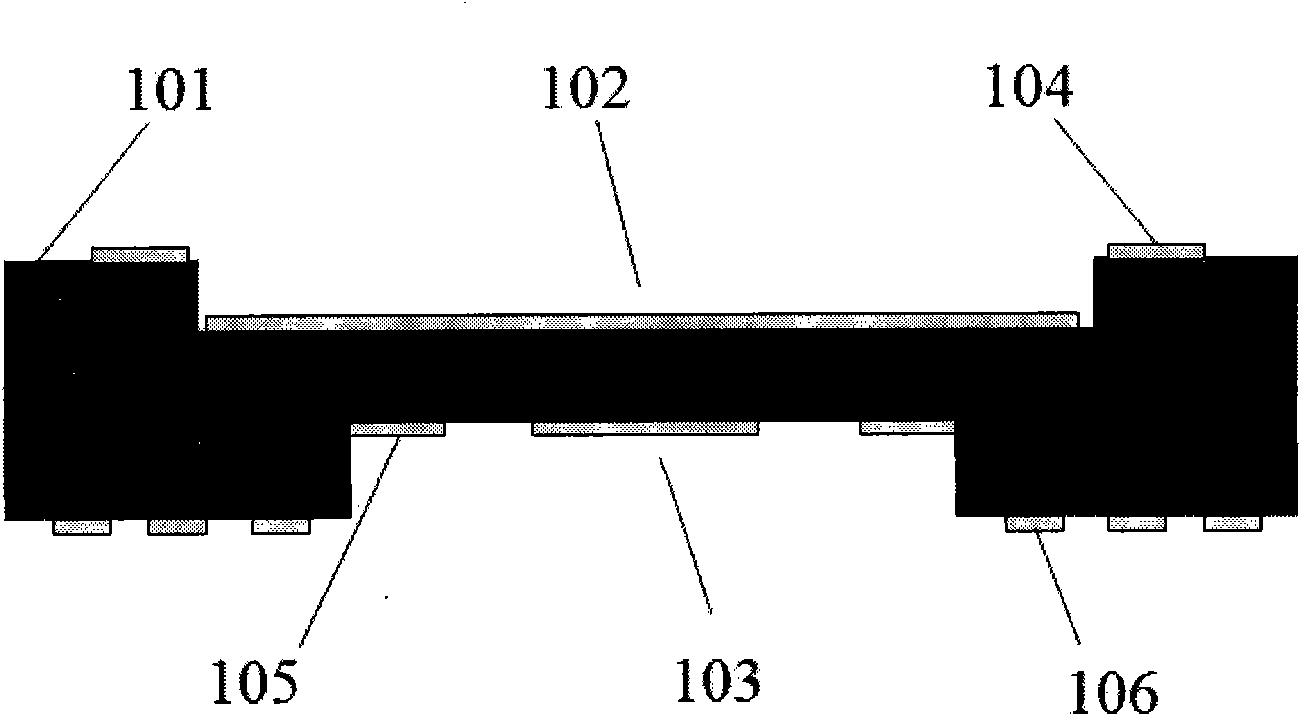
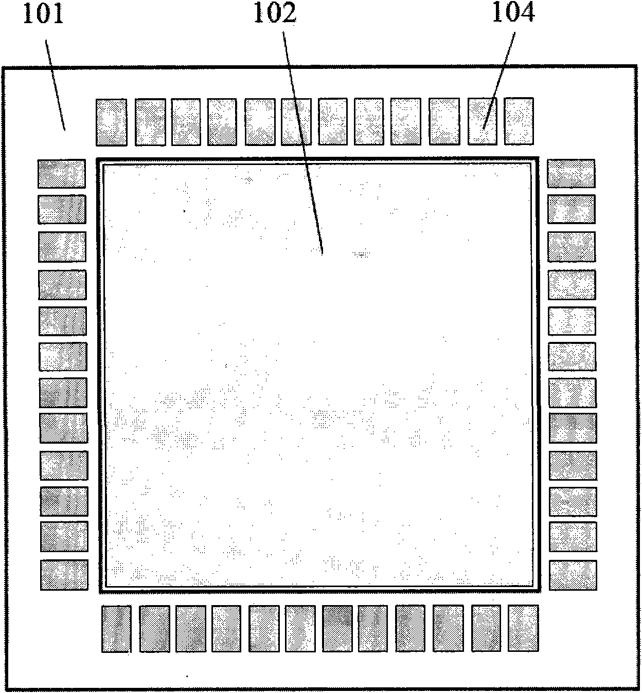
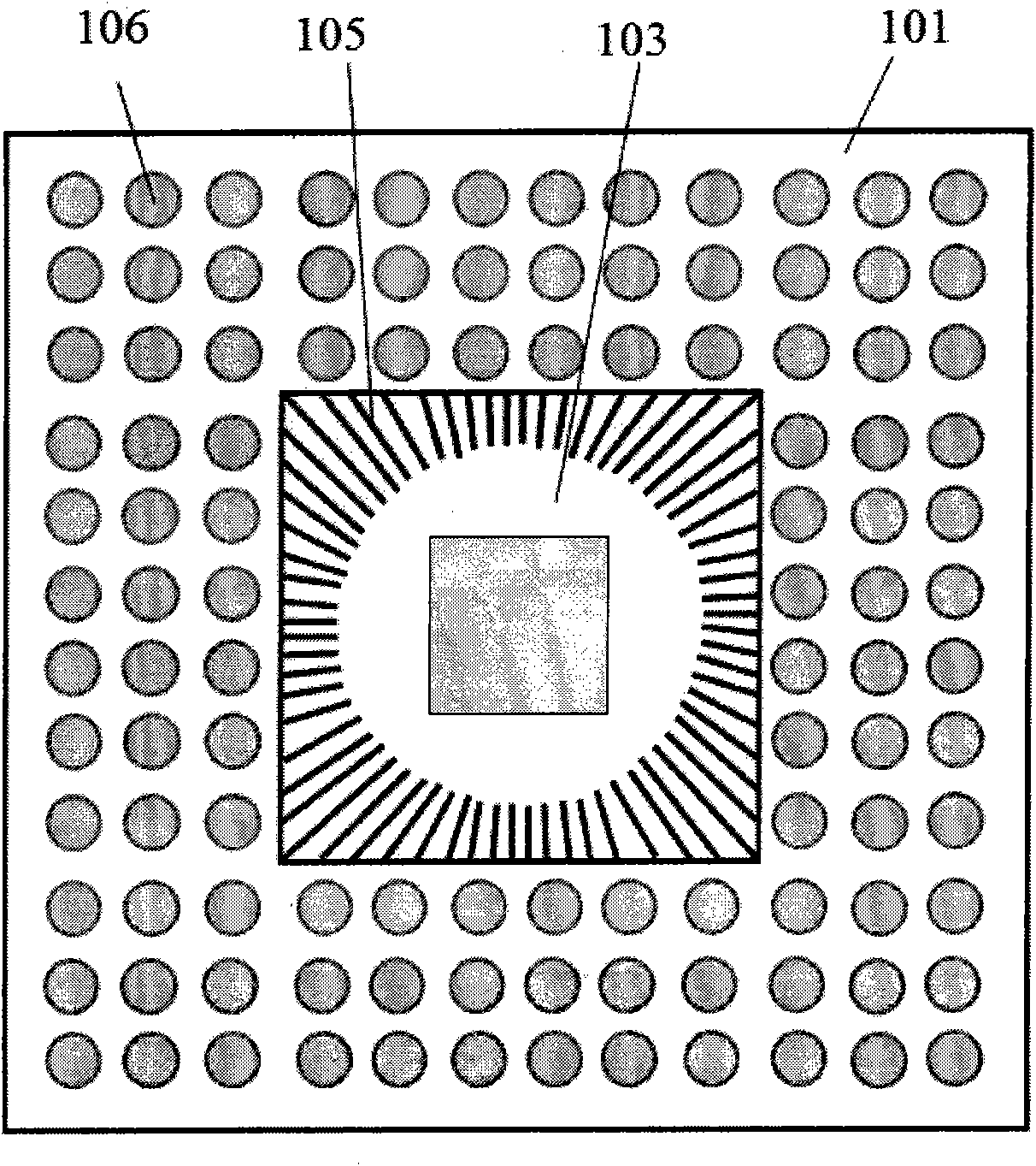
[0048] figure 1 It is a cross-sectional view of an H-shaped embedded substrate. A package substrate 101 made of a multilayer PCB has a recessed cavity 102 in the middle of the upper surface and a recessed cavity 103 in the middle of the lower surface. The package substrate in the cross-sectional view has a typical "H" structure.

[0049] exist figure 2 Among them, the recessed cavity 102 in the middle of the upper surface of the packaging substrate 101 is a large-sized cavity. The size of the cavity should be just enough to accommodate and mount large-size chips, and the depth of the cavity is equivalent to the thickness of the large-size chip, which can effectively shorten the length of the bonding wire. Wire bondin...


PUM


Abstract

The invention provides a buried substrate based multi-chip module structure for realizing three-dimensional high-density encapsulation (3D-MCM). The upper surface and the lower surface of the substrate have concave cavity structures; different chips having larger size difference are placed and wires are arranged in the cavity structures having different sizes so as to form a buried three-dimensional encapsulation structure; a plurality of chips are interconnected by using a conventional wire bonding method; a chip protection mode adopts two packing processes, namely sealing glue dropping and surrounding dam packing; a pin output form adopts a peripheral ball grid array mode; and by the concave cavity structures, the encapsulation area is reduced, the encapsulation density is enhanced, the bonded wire is shortened effectively, and the signal delay is decreased. The whole process and the surface assembling process are compatible with each other and have characteristics of simpleness and low cost. By the concave cavity structures on the upper surface and the lower surface of the substrate, the warping of the substrate is decreased and the reliability of the three-dimensional encapsulation structure is improved.

Description

technical field [0001] The invention relates to a structure and method of three-dimensional multi-chip packaging realized by using an embedded substrate. More precisely, the invention relates to a multi-chip module structure and method based on an H-shaped embedded substrate to realize three-dimensional packaging, which belongs to microelectronics packaging field. Background technique [0002] Multi-chip module (MCM) packaging is to package multiple chips on a substrate to complete certain circuit functions. On the basis of multi-chip module XY two-dimensional packaging, a three-dimensional multi-chip module (3D-MCM) has emerged in the Z direction. It stacks chips together along the Z axis to maximize packaging density and reduce package size. Three-dimensional packaging has the advantages of small size and volume, higher assembly efficiency, further shortened delay, further reduced noise, reduced power consumption, faster speed, and increased bandwidth. [0003] There ar...

Claims


Application Information

Patent Timeline
Patent Type & Authority Applications(China)
IPC IPC(8): H01L23/485H01L23/498H01L23/525H01L21/50H01L21/56H01L21/60
CPCH01L2924/15311H01L2224/73265H01L2924/15153H01L2224/48227H01L2224/32225H01L2224/92247H01L24/73
Inventor 徐高卫罗乐
Owner SHANGHAI INST OF MICROSYSTEM & INFORMATION TECH CHINESE ACAD OF SCI
Why Eureka
Try Eureka