

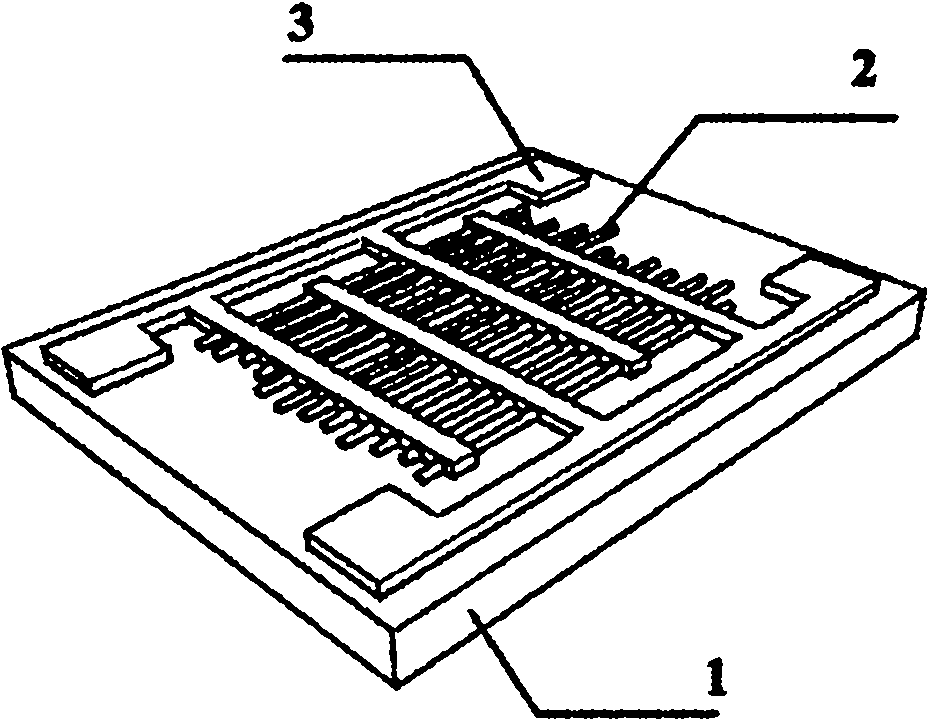
ZnSe nano-photoelectric detector and preparation method thereof
A photodetector and nanotechnology, applied in the direction of circuits, electrical components, semiconductor devices, etc., can solve the problem that the area of the switch is smaller than that of the photosensitive layer, and achieve the effects of improving contact, increasing concentration, and increasing electrical signals
- Summary
- Abstract
- Description
- Claims
- Application Information
AI Technical Summary
Problems solved by technology
Method used
Image

Examples
Embodiment 1
[0029] Embodiment 1: This embodiment is prepared according to the following steps
[0030] 1. Use acetone, alcohol, and pure water in sequence to treat SiO on the surface 2 The Si substrate of the first layer was ultrasonically treated for 15 minutes, and then dried with nitrogen gas with a purity not lower than 99%;
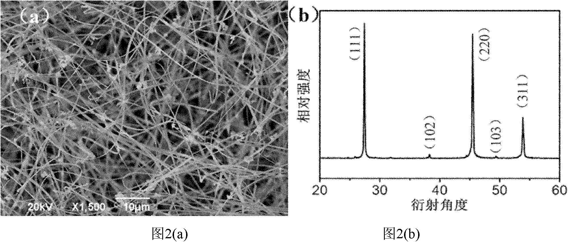
[0031] 2. According to the atomic ratio of 1%, mix and grind the doping material I with a purity of not less than 99.9% and ZnSe powder with a purity of 99.9% for 30 minutes to obtain the raw material, weigh 0.5g of the raw material and put it into Al with a purity of 99.9% 2 o 3 In the porcelain boat, place the porcelain boat in the center of the horizontal tube furnace; place a steamed gold silicon wafer 10cm away from the small porcelain boat downstream of the carrier gas. The thickness of the gold film on the evaporated gold silicon wafer is 15nm. The background vacuum in the horizontal tube furnace was evacuated to 10 by mechanical pump and molecular pum...
Embodiment 2
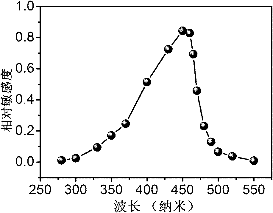
[0036] with SiO on the surface 2 Layer Si sheet is as substrate, and doping element is I, and doping concentration is 25%, adopts the preparation method identical with embodiment 1, sees in the photoresponse spectrum of ZnSe nanometer photodetector through the preparation gained. Figure 5 .
Embodiment 3
[0038] with SiO on the surface 2Layer Si sheet is as substrate, and doping element is I, and doping concentration is 50%, adopts the preparation mode identical with embodiment 1, sees in the photoresponse spectrum of ZnSe nanometer photodetector through the preparation gained. Image 6 .
PUM
 Abstract
Description
Claims
Application Information