Silicon carbide single crystal substrate

一种碳化硅单晶、基板的技术,应用在单晶生长、单晶生长、晶体生长等方向,能够解决薄膜结晶缺陷、异常生长等问题

Active Publication Date: 2011-08-24
RESONAC CORPORATION
View PDF5 Cites 13 Cited by
  • Summary
  • Abstract
  • Description
  • Claims
  • Application Information

AI Technical Summary

Problems solved by technology

[0013] The remaining adhered particles with a size exceeding the optical detection limit, which cannot be detected by conventional methods, may cause abnormal growth during epitaxial growth, etc., and there is still the possibility of causing crystal defects in the above-mentioned thin film.

Method used


Image

  • Silicon carbide single crystal substrate
  • Silicon carbide single crystal substrate
  • Silicon carbide single crystal substrate

Examples


Embodiment 1

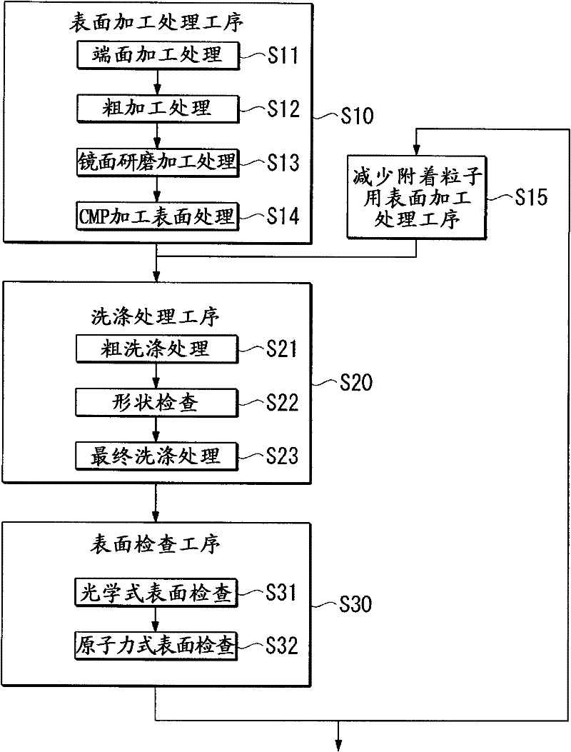
[0086] use figure 1 A silicon carbide single crystal substrate (sample of Example 1) was produced in the process of producing a silicon carbide single crystal substrate shown in the flowchart.

[0087]

[0088] First, a (0001) 8° inclined substrate of a silicon carbide single crystal substrate having a diameter of about 50 mmΦ is prepared, and a predetermined end surface processing is performed.

[0089] Next, the silicon carbide single crystal substrate is sandwiched between the upper and lower two flat stages, and the two stages are rotated facing each other while supplying abrasives, and the front and back surfaces of the above-mentioned silicon carbide single crystal substrate are shaved to adjust the thickness. Rough machining was performed to improve the flatness. As the processing abrasive grains, diamond abrasive grains were used.

[0090] Next, attach a nonwoven fabric or the like to the processed surfaces of the upper and lower flat platforms, sandwich the silic...

Embodiment 2

[0106] After the surface processing step was completed, the board was mounted on a single-sided processing machine, and the time for surface cleaning performed by supplying only pure water was set to 1 minute, and a silicon carbide single crystal substrate was performed in the same manner as in Example 1 ( Embodiment 2 sample) making.

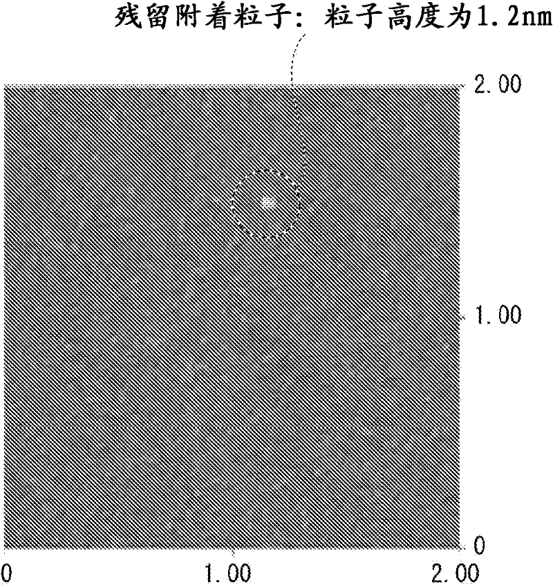
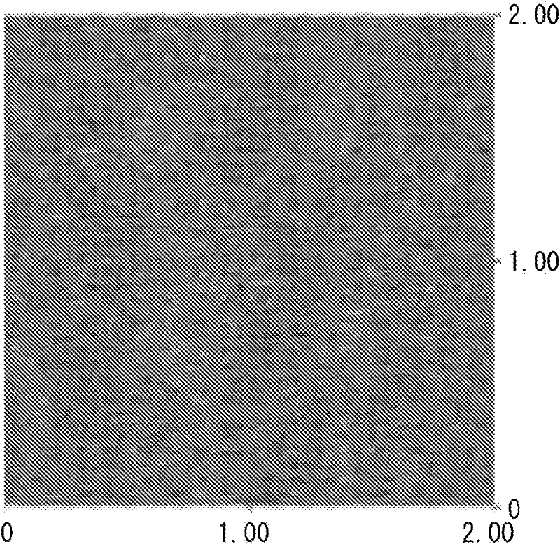
[0107] After adjusting the pH value of the surface of the silicon carbide single crystal substrate to 1 using an abrasive containing diamond abrasive grains and an abrasive cloth impregnated with a pH adjuster, and performing a surface treatment process (mirror polishing treatment) for reducing attached particles , and repeatedly carry out the above-mentioned washing treatment process. Thereafter, the surface inspection process is performed again.

[0108] In the dark-field visual inspection of silicon carbide single crystal substrates and optical surface inspections using SurfScan (manufactured by Tencor Corporation), no surface flaws, cloudi...


PUM

PropertyMeasurementUnit
heightaaaaaaaaaa
roughnessaaaaaaaaaa
roughnessaaaaaaaaaa

Abstract

Provided is a silicon carbide single crystal substrate having adhered particles that cause crystal defects removed therefrom and has high surface cleanliness. A silicon carbide single crystal substrate wherein the density of first adhered particles having an adhesion height of 100 nm or more on one surface of the substrate is one particle / cm2 or less, and the density of second adhered particles having an adhesion height of less than 100 nm on such surface of the substrate is 1500 particles / cm2 or less is used.

Description

technical field [0001] The invention relates to a silicon carbide single crystal substrate, in particular to a silicon carbide single crystal substrate with high surface cleanliness. [0002] This application claims priority based on Patent Application No. 2008-252731 for which it applied in Japan on September 30, 2008, The content is used for this application. Background technique [0003] In recent years, silicon carbide (SiC) single crystal materials have been expected as semiconductor device materials due to their excellent semiconductor characteristics of high power density and low loss. In particular, it is attracting attention as a future power electronic semiconductor device. [0004] A semiconductor device is generally formed by epitaxially growing a plurality of semiconductor layers on one side of a semiconductor substrate. Since the above-mentioned semiconductor layer is a thin film, it is desirable that one side of the above-mentioned semiconductor substrate is...

Claims


Application Information

Patent Timeline
Patent Type & Authority Applications(China)
IPC IPC(8): H01L21/304B24B37/00
CPCH01L21/02008H01L21/02052H01L21/02024B24B37/04H01L21/30625H01L29/1608C30B29/36Y10T428/24372H01L21/304B24B37/00C03B33/00
Inventor 坂口泰之
Owner RESONAC CORPORATION
Why Eureka
Try Eureka