In chamber sodium doping process and system for large scale fabrication of CIGS based thin film photovoltaic materials

A photovoltaic material and composite film technology, applied in photovoltaic power generation, metal material coating process, vacuum evaporation plating, etc., can solve the problems of long-term use, poor film reliability, and difficulty in mechanically integrating films with each other, and achieve simplification. Effect of doping process

Inactive Publication Date: 2011-08-31
CM MFG
View PDF7 Cites 12 Cited by
  • Summary
  • Abstract
  • Description
  • Claims
  • Application Information

AI Technical Summary

Problems solved by technology

Similar limitations exist for the use of thin-film technology in the manufacture of solar cells
That is, performance is often poor
In addition, membrane reliability is often poor and cannot be used for long periods of time in traditional environmental applications
Often, thin films are difficult to mechanically integrate with each other
In addition, the integration of the electrode layer and the overlying absorber layer (overlying absorber layer) formed on the sodium-containing substrate is also problematic, especially for mass production

Method used


Image

  • In chamber sodium doping process and system for large scale fabrication of CIGS based thin film photovoltaic materials
  • In chamber sodium doping process and system for large scale fabrication of CIGS based thin film photovoltaic materials
  • In chamber sodium doping process and system for large scale fabrication of CIGS based thin film photovoltaic materials

Examples


Embodiment Construction

[0014] The present invention generally relates to photovoltaic materials and methods of production. More specifically, the present invention provides a method and structure for fabricating thin film solar cells. By way of example only, the present method includes indoor sodium doping based on a large-scale batch system for the production of chalcopyrite-structured thin film photovoltaic cells, but it should be recognized that the present invention may have other configurational designs.

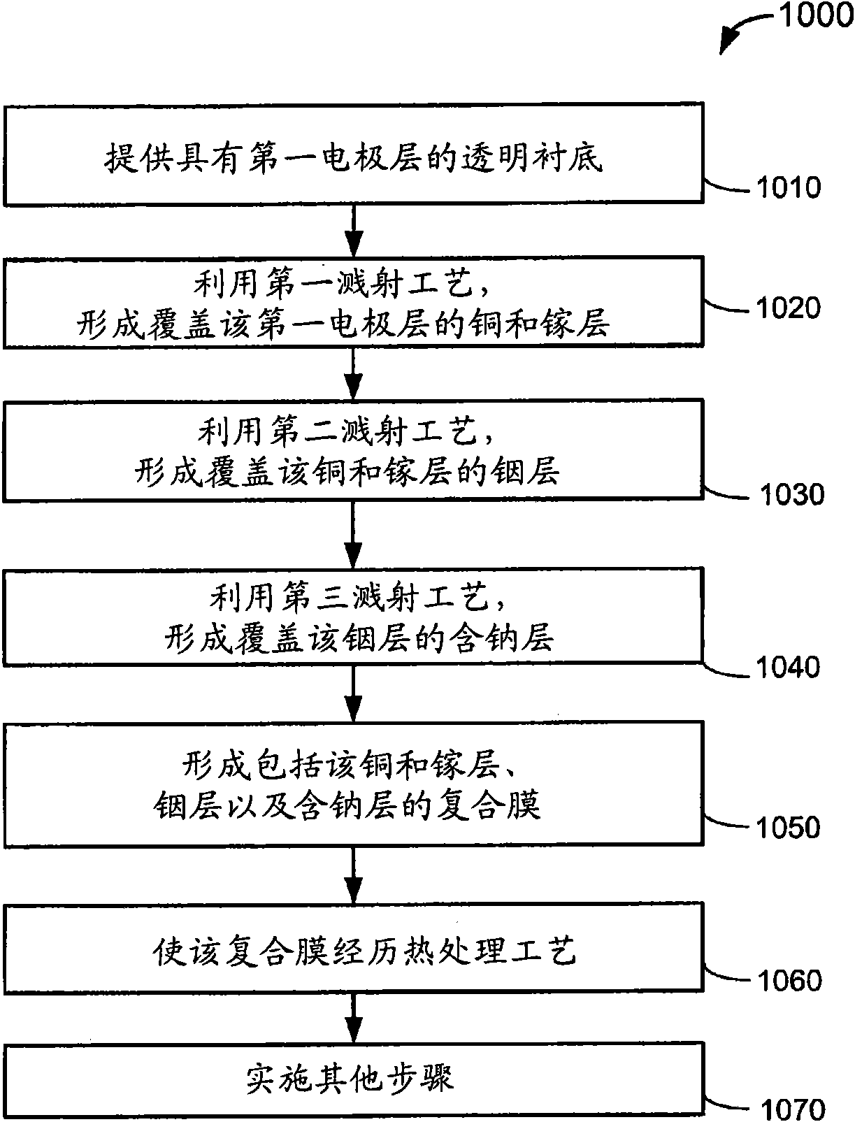
[0015] figure 1 is a simplified flowchart illustrating a method of fabricating a thin film photovoltaic cell according to one embodiment of the present invention. This diagram is merely an example, which should not unduly limit the scope of the claims appended hereto. Method 1000 includes the following processes:

[0016] 1. Process 1010 for providing a transparent substrate covered with a first electrode layer;

[0017] 2. Process 1020 for forming copper and gallium layers covering the f...


PUM


Abstract

The invention relates to in chamber sodium doping process and system for large scale fabrication of CIGS based thin film photovoltaic materials. A method of processing a photovoltaic materials using a sputtering process including providing at least one transparent substrate having an overlying first electrode layer. The method further including forming an overlying copper and gallium layer using a first sputtering process within a first chamber from a first target including a copper species and a gallium species. Additionally, the method includes forming an indium layer overlying the copper and the gallium layer using a second sputtering process within the first chamber from a second target including an indium species. The method further includes forming a sodium bearing layer overlying the indium layer using a third sputtering process within the first chamber, thereby forming a composite film including the copper and gallium layer, the indium layer, and the sodium bearing layer. Furthermore, the method includes subjecting the composite film to at least a thermal treatment process to form a chalcopyrite absorber layer comprising copper, indium, gallium, and sodium therein.

Description

technical field [0001] The present invention generally relates to photovoltaic materials and methods of production. More specifically, the present invention provides methods and structures for fabricating thin film solar cells. Merely by way of example, the present method includes in-chamber sodium doping for the production of chalcopyrite structured thin film photovoltaic cells on a large scale batch system basis, but It should be realized that the invention is capable of other structural designs. Background technique [0002] From the beginning, humans have struggled to find ways to harness energy. Energy comes in forms such as petrochemicals, hydroelectric, nuclear, wind, biomass, solar energy, and more basic forms such as wood and coal. Over the past century, modern civilization has relied on petrochemical energy as an important source of energy. Petrochemical energy sources include gas and oil. Gas includes lighter forms such as butane and propane, and is commonly ...

Claims


Application Information

Patent Timeline
Patent Type & Authority Applications(China)
IPC IPC(8): C23C14/34C23C14/58C23C14/16H01L31/18
CPCH01L31/18H01L21/02491H01L21/02579H01L21/02568H01L31/022425H01L31/03923H01L27/1423H01L21/02614H01L21/02631H01L31/0322Y02E10/541
Inventor 罗伯特D·维廷
Owner CM MFG
Why Eureka
Try Eureka