Preparation technology for increasing effective photosensitive area of photoelectric material

A technology of photosensitive area and optoelectronic materials, applied in microlithography exposure equipment, circuits, electrical components, etc., can solve the problems of difficulty, restricting the development of solar cells, and high processing costs

Inactive Publication Date: 2011-08-31
CHANGCHUN UNIV OF SCI & TECH
View PDF2 Cites 5 Cited by
  • Summary
  • Abstract
  • Description
  • Claims
  • Application Information

AI Technical Summary

Problems solved by technology

[0003] In the current preparation of photoelectric materials, especially the preparation process of solar cells, the main design ideas are to reduce reflection, increase light irradiance and improve absorption efficiency. The realization of related technologies and process requirements are

Method used


Image

  • Preparation technology for increasing effective photosensitive area of photoelectric material
  • Preparation technology for increasing effective photosensitive area of photoelectric material
  • Preparation technology for increasing effective photosensitive area of photoelectric material

Examples


Embodiment Construction

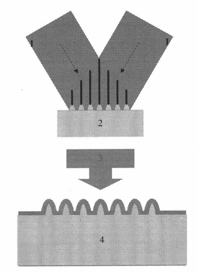
[0017] As shown in the figure, the present invention adopts the preparation technology of increasing the effective photosensitive area on the photoelectric material per unit size. Firstly, two beams of coherent light 1 in the laser interference lithography system are used to interfere on the surface of the substrate 2 material to obtain a micro-nano-scale periodic structure, and the structure is subjected to semiconductor doping treatment 3 to obtain a large surface area per unit size. Micro-Nano Periodic P-N Section Materials 4.

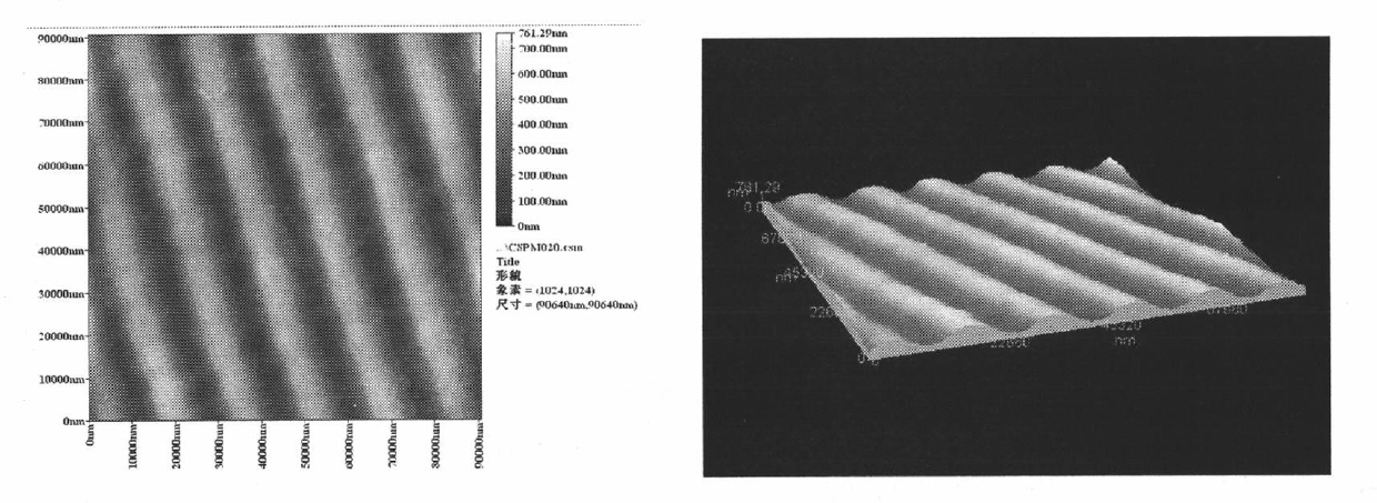
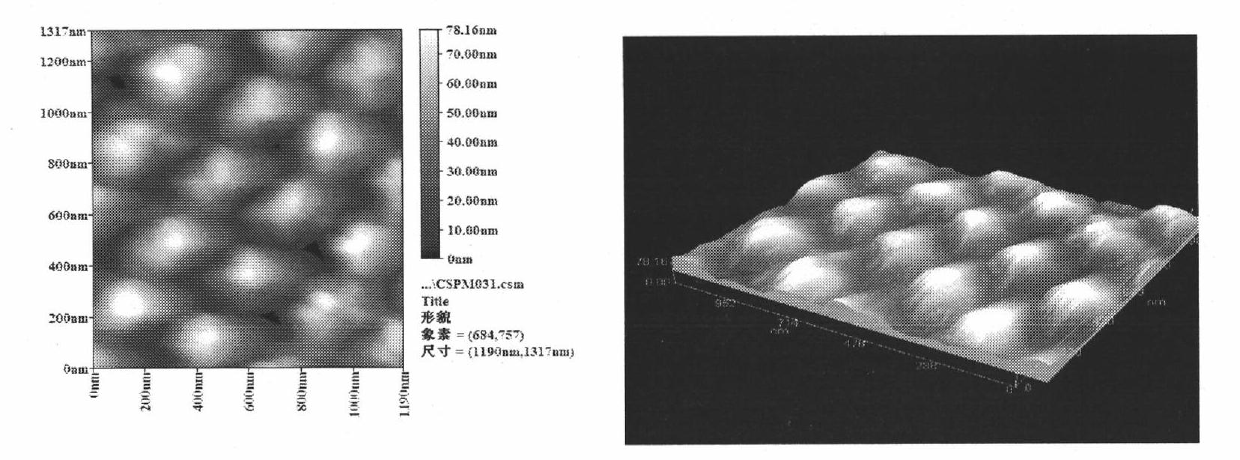
[0018] The above-mentioned laser interference exposure can be either two-beam single exposure to obtain a periodic grating structure, or double-beam double exposure or multi-beam exposure to obtain a three-dimensional columnar, spherical or depressed dot array. The characteristic size, period and pattern of the micro-nanostructure can be tuned by controlling the polarization and incident angle of the interference.


PUM


Abstract

The invention discloses a preparation technology for increasing the effective photosensitive area of a photoelectric material or a photoelectric element. The principle of the preparation technology comprises the following steps of: controlling the quantity of exposed light beams, light beam polarization and an incident angle to obtain a micro-nano structure with different periods and characteristic sizes by laser interference photoetching; and increasing the real effective area of a P-N junction within unit area on the structure by semiconductor doping. Because the photoelectric material or the photoelectric element is manufactured by using the technology and a method, the effective photosensitive area can be increased on a large scale within the unit area, and then light absorption rate is improved; the application prospect of the technology is wider due to the properties of self cleaning and anti-reflection of the micro-nano structure; the technology is particularly applied to the field of solar batteries; and conversion efficiency is improved on a large scale.

Description

technical field [0001] The present invention relates to a preparation technology for increasing the effective photosensitive area of ​​photoelectric materials or components, in particular to a technology and method for making a P-N junction structure with high efficiency and large effective photosensitive area, which can be applied to advanced manufacturing such as solar cell processing, New energy and new materials fields. technical background [0002] The principle of the preparation technology to increase the effective photosensitive area of ​​photoelectric materials or components is to use laser interference lithography to obtain micro-nano-scale structures with different periods and feature sizes by controlling the number of exposure beams, beam polarization and incident angle, and In this structure, semiconductor doping is used to finally increase the actual effective photosensitive area of ​​the P-N junction within a unit size. Using this technology and method to man...

Claims


Application Information

Patent Timeline
IPC IPC(8): H01L31/18G03F7/20
CPCY02P70/50
Inventor 徐佳王作斌翁占坤宋正勋胡贞赵乐袁安刚
Owner CHANGCHUN UNIV OF SCI & TECH
Why Eureka
Try Eureka